‘In the ever-evolving world of optoelectronic devices, perovskite materials have emerged as revolutionary components, with a theoretical stake in the manufacture of light-emitting diodes (LEDs) and quantum dots (QDs). At least that is what the wealth of research on the material suggests. These materials promise to transform modern lighting and display technologies with their exceptional electronic and photonic properties. Perovskite QDs, are supposed to have superior color purity and tunable properties, particularly beneficial for developing high-performance LEDs and vibrant displays. There’s really only one company of significance that has any real insight into commercial viability of perovskite in the industry, Helio Display Materials out of the UK.
So, what are we to think of perovskite strategies in the display industry? Maybe they are non-existent, or maybe they are too experimental for the powers that be, more focused as they are in next gen display technologies that have been in the works for decades. Maybe it is because the existing display materials market is primarily driven by materials scientists, and perovskite is a chemists dream. Perovskites are relatively easy to synthesize in the lab with their unique crystal structure giving them a wide range of properties, including high electrical conductivity, magnetism, and photovoltaic capabilities.
Or, maybe they are just too unstable or need to be bound with heavy metals, negating any obvious advantages by skirting the demands of RoHS. Whatever the reasons are for a lack of a perovskite strategy in major display manufacturers won’t make the materials go away or reduce the body of research into them for displays.
Historical Background of Perovskite Materials
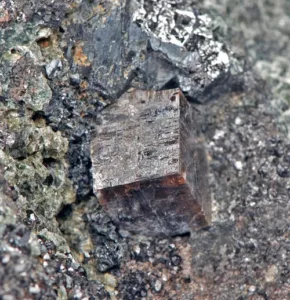
The history of perovskites dates back to 1839 when the mineral CaTiO3 was discovered in the Ural Mountains by Gustav Rose and named after the Russian Count Lev A. Perovski. Initially recognized as metal oxide minerals, the scope of perovskites has broadened immensely, especially with the synthesis of lead halide compounds exhibiting similar structures. Over the years, the inclusion of organic components led to the development of hybrid perovskites, which have since played a pivotal role in advancing optoelectronic applications. The adaptable composition and structure of perovskites, coupled with their ability to form high-quality crystals at low temperatures, continue to drive research and innovation across various technological domains.
Perovskite LEDs and QDs
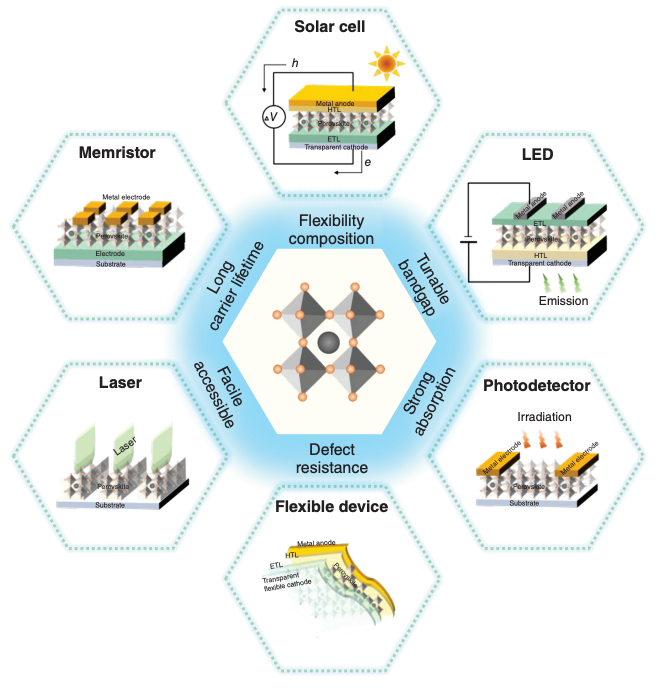
Perovskite LEDs (PeLEDs) genuinely represent an opportunity in lighting and display technology. These LEDs are characterized by high external quantum efficiencies (EQEs), which have already surpassed 20%, making them formidable competitors in next-generation display technologies. The recent integration of perovskite QDs into thin-film transistor circuits has further led to the development of active-matrix perovskite displays. These displays not only maintain a high EQE of 23.6% at a brightness level of 300 cd/m² but also showcase the potential for large-scale application in sophisticated display technologies.
Despite these impressive performance metrics, the operational stability of PeLEDs remains a significant challenge, primarily due to environmental factors, material degradation, and operational stresses that lead to phase separation and ion migration. Addressing these challenges is essential for extending the operational lifetime and maintaining the efficiency of these devices over time. Several strategies are being pursued:
- Nanoengineering: Techniques to improve the material properties at the microscopic level are being developed. These include engineering the perovskite material at the nanoscale to enhance its environmental resistance and electronic properties.
- Device Encapsulation: Proper encapsulation is crucial to protect the sensitive materials from moisture, oxygen, and other environmental factors. Advanced techniques in this area can significantly extend the lifespan of the devices.
- Surface and Interface Passivation: Reducing defects in perovskite films through passivation helps mitigate non-radiative recombination centers, thereby improving the photophysical properties and operational stability.
- Interfacial Treatment: Optimizing the interfaces within the LED structure can reduce ion migration and bias-induced phase separation, promoting uniform charge distribution and preventing ion accumulation.
If you look at the challenges facing wider acceptance and adoption of perovskite materials in the display industry, you are looking at the general obstacles for any new display material, no matter how good, to find a path into end products. The things that deliver color and light, and the things that direct that color and light, are all layers of complexity, positioning, and some level of religious fervor. Nothing in a display exists, or is evaluated, in isolation. So, PeLEDs and perovskite QDs are trying to find an insertion point into one of many layers of a display build. That would be great if it was just a case of swapping one layer for another, new one, but that’s not displays are manufactured.
As I said earlier, the body of research on perovskite in optoelectronics is growing, and is quite impressive in its own right. It is not going to disappear from conversation in the display industry, but when you consider that Helio Display Materials only managed to go into pilot production of its perovskite for displays in the first quarter of this year, and that the company’s fundraising is a fraction of what has gone into any number of MicroLED startups, then you might think, what is all the fuss about? Perovskite is never going to cut it in the display industry.
Sure, it never comes up in conversations about LCD, OLED, and MicroLED, but it may just become something that finds itself into the mainstream comparisons. Not until there are actual PeLED display products in the hands of consumers, or any with perovskite QDs. But, that may be the failure of display industry supply chains to include it, and not a failure of the technology to deliver on its promise.
Unfortunately, without the former, the latter cannot evolve. That is a sad reflection on innovation in displays and broader opportunities to expand the frontiers of what’s possible.
Reference
Li, H., Feng, Y., Zhu, M., Gao, Y., Fan, C., Cui, Q., Cai, Q., Yang, K., He, H., Dai, X., Huang, J., & Ye, Z. (2024). Nanosurface-reconstructed perovskite for highly efficient and stable active-matrix light-emitting diode display. Nature Nanotechnology, 1–8. https://doi.org/10.1038/s41565-024-01652-y
Zhang, Q., Zhang, D., Cao, B., Poddar, S., Mo, X., & Fan, Z. (2024). Improving the Operational Lifetime of Metal-Halide Perovskite Light-Emitting Diodes with Dimension Control and Ligand Engineering. ACS Nano, 18(12), 8557–8570. https://doi.org/10.1021/acsnano.3c13136