
In the good old days of LCD manufacturing the optimal size of a display panel and the mother glass size was something that could easily be determined by a simple spreadsheet.

Today this relationship still exists, but the number of options has increased sharply as the mother glass size, the fab generations, as well as the display panel sizes have grown over the years.
The drive to larger substrate sizes seemed inevitable. As long as the yields and cycle times remain somewhat equal, larger substrates yield more display panels at a lower manufacturing cost. While the capital investment into larger substrate plants increase as a total number, the capital investment per substrate area has decreased sharply over the years, as Corning has shown.
As a consequence, manufacturers have fought for a long time to make their products on the largest substrate possible. This strategy allowed cost competitive manufacturing of TV panels, creating the LCD manufacturing business we have today.
 Source: Nikon
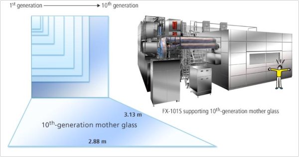
This was until Sharp opened its Gen 10 plant at a time of economic downturn. With falling TV panel demand and high fixed operation cost, Sharp accumulated drastic losses, pushing the company to the edge of bankruptcy. For the first time a larger substrate size did not automatically translate into business success. A valuable reminder that it is not only important what you do, but also when you do it.
Today, several companies are talking about Gen 10 and Gen 10.5 LCD Fabs to gain a cost advantage in the display panel business. So it came as somewhat of a surprise when Digitimes quoted the Korea Money Today newspaper as a source saying that LG is thinking about the investment in a Gen 9 LCD Fab instead of a Gen 10, to compete with Chinese and Japanese competitors.
While there is no way to verify this report, as LG is just not commenting on this speculation, it may just be an idea from the analyst instead of actual LG insider information. Or is it actually possible that LG would do such a thing?
The article continues to suggest that these new factories are actually planned as hybrid plants that are capable of producing LCD as well as OLED panels. While OLED developers always claimed that LCD Fabs will work well as the basis for OLED manufacturing, this may be the first new factory that would be built to manufacture both technologies side by side. There is no further discussion if the capacity would be split or can be shifted either way, so it is impossible to understand the consequences for the manufacturing process and ultimately the profitability of such a plant.
So why would LG shift its investments to build a FAB using smaller substrates and add technology complexity at the same time? This looks on the first glance like a double disadvantage. However, LG and Samsung as well have always seen OLEDs as the ultimate challenger of the LCD technology. From this perspective this could mean that they are willing to gamble big on the breakthrough of OLED in the coming years, or they are uncertain on the size distribution of the future LCD panel demand.
Either way, LG may be thinking about a different investment strategy compared to the rest of the industry. So if there is any truth to this press statement, I would guess that LG managers are quite busy right now, running as many scenarios as possible. We can just sit down and relax until the real LG press release tells us, what the company will do. – Norbert Hildebrand