We don’t often talk about Electronic Design Automation (EDA) tools for displays, but they are essential to be able to model new designs and new processes. Probably the premier supplier of backplane modeling tools is Silvaco. According to Amit Nanda, the VP of Global Marketing at Silvaco, “one or more of the company’s modeling and simulation tools are used by 90% of the LCD industry.” That’s a pretty high penetration rate.

![]()
We recently had a chance to talk to Nanda about their latest tool and learn a bit more about backplane design for displays. The new tool is called Clever LCD and is an extension of the previously released Clever simulation tool.
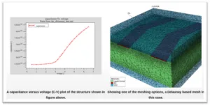
One of the most important parameters to model in the display backplane is the pixel and parasitic capacitance, which has a big impact on how you drive the display and how fast you can turn the pixel on and off. Clever develops a 3D model of the TFT device structure which includes specifying the permittivity (ability to store electrical energy) of the various materials, including the liquid crystal material. For many applications, Clever LCD offers sufficient capacitance extraction accuracy for most LCD/OLED design needs. Besides electrical analysis, Clever LCD can also be used to evaluate the optical performance of a display.
“Within the last few years, our customers have been asking for more accuracy and precision in the capacitance modeling,” noted Nanda. He thinks that the trend toward higher density displays is one factor driving this need. Another is the advancement in backplane processing that may drive changes device layers and structures in an effort to reduce cost.
“What the new Clever LCD tool does is make the permittivity of the materials a function of voltage instead of a fixed value. This means much better capacitance estimation is possible under real operational conditions,” explained Nanda. Japan Display Inc. (JDI) is the first company to adopt the tool after a rigorous evaluation.
Makoto Watanabe, General Manager of the Technology Promotion Department of the Technology Division of Japan Display, stated, “Clever LCD makes it possible for us to accurately and quickly calculate the liquid crystal capacitance, which is a dominant part of the overall pixel, and other parasitic capacitance simultaneously. Therefore, we expect to realize even more precision in our designs compared to that attained by conventional methods.”
Clever and Clever LCD are 3D simulation tools that use a field follower or field solver model. This model is employed for fine-scale, i.e. pixel-scale design needs. For display-scale design needs, like understanding the impact of address bus lines, the company’s “rule-based” Hipex simulator is used.
Nanda explained that there are many steps to developing models and simulators for display backplane design. The process starts by developing a 3D model of the design circuit using the company’s Technology Computer-Aided Design (TCAD) tool called Victory. This integrates the design of the transistors and other electrical elements, materials parameters and even the fab design process parameters. This tool means designers can change the width or length of a transistor channel, change material properties and fabrication process parameters in lithography, etch, implant or other processes – all to see the impact on device performance. Note that we are talking about the design of the backplane here so the output is typically an I-V curve.
To be sure the model is accurate it is validated or calibrated against actually fabricated devices with known process and material parameters and measured I-V data. This is crucial to allowing the model to run “what if” scenarios.
A simulation then assembles a number of modeled elements into a circuit – a display – to understand performance at this level. These simulations are based on a Simulation Program with Integrated Circuit Emphasis (SPICE) methodology and these models are created by using a Silvaco tool called Utmost IV. Special SPICE compact models such as RPI are used for a-Si TFT and UOTFT for organic and oxide TFTs.
The circuit schematic also serves as the input for the Clever/Clever LCD or Hipex capacitance analysis. This is sort of clear in the diagram below.
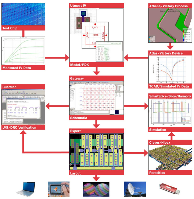
Nanda stressed that they have tools for all stages of design from TCAD to signoff. For example, additional tools besides those mentioned above include:
- Schematic and layout tools for circuit design creation
- SPICE simulation tools including capability for full display and hysteresis simulation
- Physical verification tools for LVS and DRC checks
Nanda concluded by noting that Silvaco’s TCAD background and strength in meshing and solvers enables good convergence and makes it possible to simulate very complex structures in a minimum amount of time. Silvaco’s product suite is used for design of both thin-film transistor (TFT) LCD displays and organic LED (OLED) displays including a-Si, LTPS, Zn-Oxide and organic material-based backplane design.
– Chris Chinnock