Who is Plessey Semiconductor, you may ask? This does not sound like a display company, but it is. Based in Plymouth, UK, Plessey Semiconductor is developing wafer-scale microLEDs ideally suited for AR, VR and HUD applications, but with the right mass-transfer technique, may also be suitable for larger, direct-view displays as well.

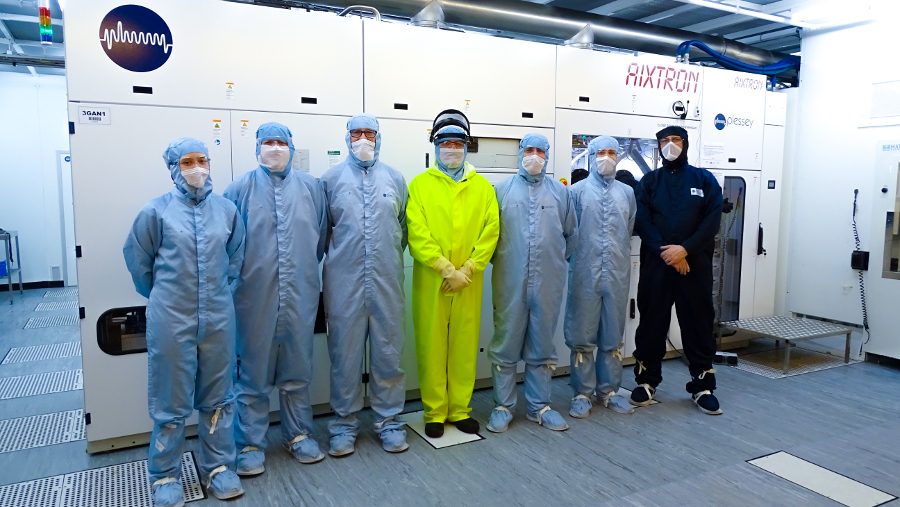
On a recent visit to their facility I received a full tour of their factory. It is impressive. And one of the best things they have going it that nearly all the processing is done in-house allowing for more control and faster development times.
![]()
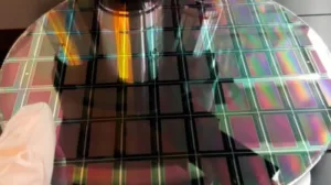
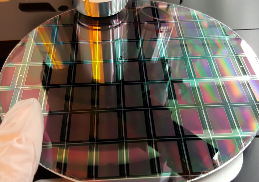
So what is Plessey’s approach? It all began with buffer layer technology developed by UK-based Cambridge University that allows the growth of GaN on top of silicon wafers. These buffer layers are crucial to allow a transition from one crystal structure to the other. By eliminating the stress between these two materials systems, Plessey is able to fabricate GaN-on-Silicon wafers that have no bowing or potato-chip distortions. The resulting wafers must be extremely flat to be used with photolithographic stepper machines to pattern the wafer into microdisplay devices. This is a big deal and key IP that the company controls via its license from Cambridge University.
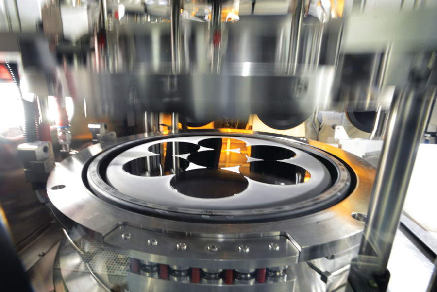
There are lots of these buffer layers – dozens, maybe more than 100 that must be first deposited on the silicon wafer. Then, the wafer moves to MOCVD machines to produce the GaN layers needed to create the microLEDs that emit blue or green light. OK, so far so good. But these microLEDs need to be driven with current to produce light – i.e., they need a backplane.
Most developers of monolithic microLEDs are using silicon to create the backplane. Unfortunately, development of backplanes can be a very costly undertaking, so Plessey is trying to leverage backplanes developed for LCOS microdisplays. The issue here is that LCOS displays are voltage-driven while microLEDs want to be current-driven. I am not sure how simple it is to adapt a voltage-driven design to current-driven implementation, but Jasper Display has done this for one of their devices (a 0.7” FHD device). What is a little unclear is the best design of a backplane for AR, VR or HUD applications. This lack of a clear spec and the money to design and develop one is a key factor holding back a more rapid development cycle of monolithic microLEDs.
But I digress. To finish the process, the GaN microLEDs on the silicon wafer must now be flipped over (microLEDs facing down) and bonded to the backplane wafer with very precise alignment. The silicon wafer that holds the microLEDs is now removed to expose the microLEDs.
So why process GaN on silicon instead of sapphire, the current method of mainstream fabrication? There are two main reasons. One is the mass production scale that silicon allows with wafer sizes as large as 12 inches. Plessey is mostly processing 6” wafers today, but the equipment is capable of 8”. That’s a big step up from the 2” and 4” substrates currently used with sapphire GaN. As we know from flat panel manufacturing, size can have a big impact on reducing costs.
Secondly, silicon is a much better thermal conductor compared to sapphire. That means the substrates can have more uniform thermal control in the manufacturing process leading to much lower distribution of wavelengths and turn-on voltages. This is critical for monolithic microLEDs as you can’t bin the devices – they all better be in spec or that device is no good. Better thermal conductivity will also allow the devices to operate at lower temperatures for a given output level, helping improve lifetime, or they can run at even higher brightness levels. Very high brightness is especially critical for daytime use in AR and HUD applications.
Plessey has made a considerable investment in new processing equipment to be able to manufacture displays in house. The only part that is outsourced is the backplane. Competitors sometime rely on University fabrication facilities which can take months to complete a fabrication run. Vertical integration allows displays to be completed in about 2-3 weeks.
Plessey is currently working with a number of customers developing displays mostly for AR and HUD applications. But they are starting to investigate mass-transfer technology that might allow them to tackle direct-view applications like video walls or even TVs.
Many challenges remain in the commercialization of microLED-based products, whether microdisplay monolithic type or larger direct-view type. But Plessey’s GaN-on-silicon approach is one very promising area that addresses both performance and cost. I am sure we will be hearing more from this company in the future.