As the display industry widely awaits the launch of QD-OLEDs by Samsung in 2021, an obvious question in everyone’s minds is – what’s next? What does the display roadmap look like in the premium TV segment? Having a blue OLED as the backlight can limit the ultimate brightness, while microLEDs continue to be very expensive to manufacture and self-emissive Cd-free EL-QDs may not be ready for mass production for some time. Well, the answer might very well be ‘QNED’- Quantum Nano Emitting Diode display technology.

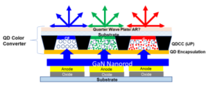
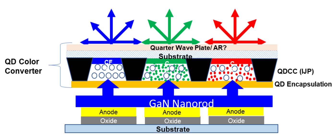
Samsung is reportedly working on QNED technology in which GaN-based blue light emitting Nanorod LEDs will replace OLED as the blue light source. The advantages of the QNED structure over QD-OLED include higher efficiencies, improved brightness, longer lifetimes and elimination of burn in issues that have been associated with OLEDs. Additionally, since GaN Nanorods are expected to be far more stable than OLED materials, thin film encapsulation will not be required on top of the GaN Nanorods. Quantum dots will still be used in the color conversion process for the red and green pixels since the native emission color of the Nanorods is expected to be blue.
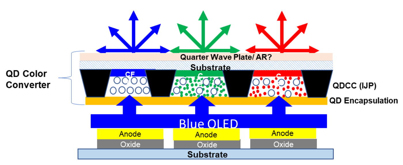
A simplified cross section of the QD-OLED and QNED device is shown below where the OLED is replaced by the GaN Nanorod LED.
QD OLED
QNED
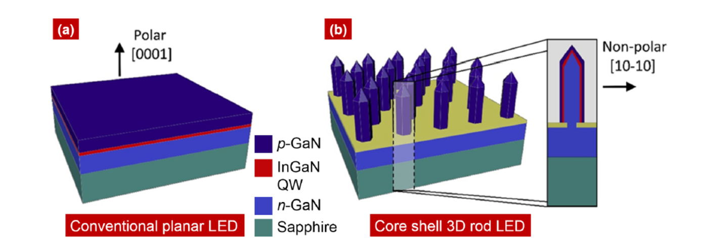
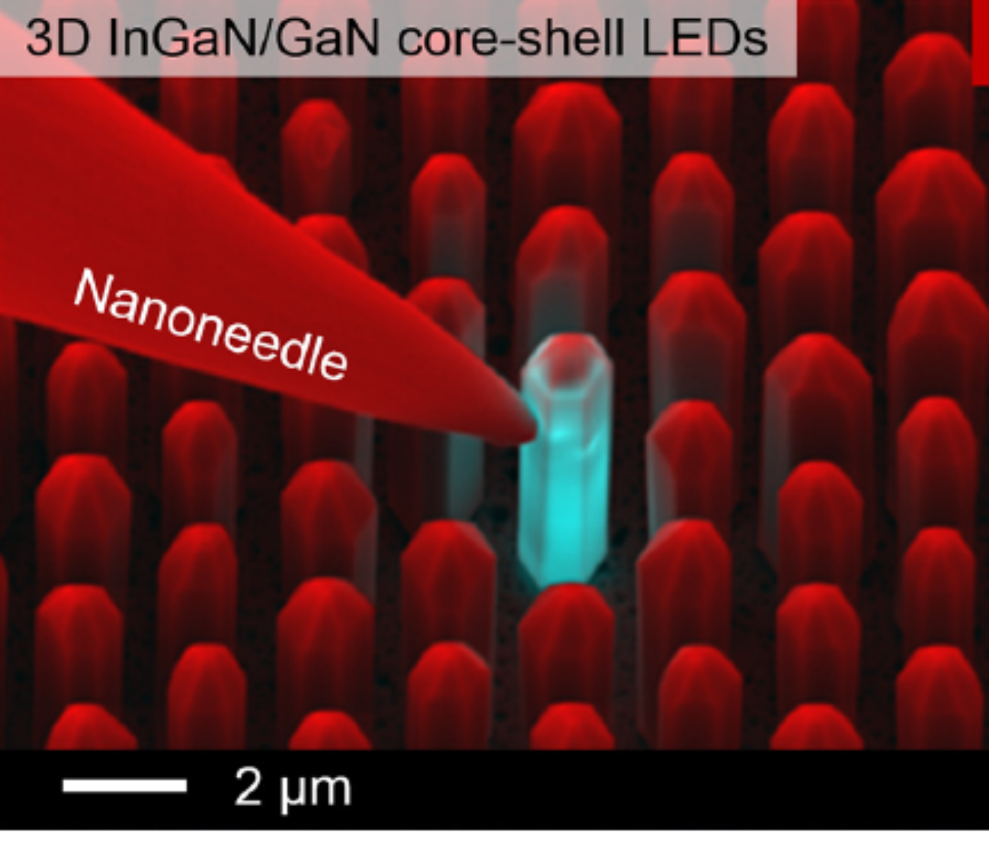
Blue GaN Nanorod LEDs: Why Nanorods? – Nanorod structures possess some key features, which potentially are very attractive for use in this application. GaN nanorods with high aspect-ratio and large surface-to-volume ratio can dramatically reduce the dislocation density in the upper part of the nanorods. The light extraction efficiency is expected to increase owing to the non-planar geometry of nanorods. A substantial benefit of the nanostructure is the realization of a core shell structure.
Most promisingly, core/shell nanorod structures in which the InGaN/GaN multi-quantum wells (MQWs) grow on the whole cylindrical surface of the nanorods are suggested to be able to effectively increase the active area by a factor of about 4* aspect ratio (as high as 10 X larger emitting surface area) and, as a consequence, increase the total light intensity of the same substrate area. Furthermore, since the dimensions of these structures are small, Nanorods can be blanket coated over the bottom electrode and the TFTs can be used control the pixel switching. In essence, a “self-emissive” blue nanoLED pixel can be made and the resolution of such a display in theory will be limited by only the underlying TFT layer.
QNED structure: The QNED structure consists of the following:
- Backplane
- Blue GaN Nanorod LEDs
- Quantum Dot Color Conversion
- Backplane: For TV applications, the backplane will likely be be high mobility IGZO oxide TFTs which is same as the current oxide TFTs used for manufacturing OLED TV panels. Therefore, Samsung’s existing (or to be installed) QD-OLED equipment can be used to manufacture the backplane.
- Blue GaN Nanorod LEDs: This includes two parts
- Nanorod Fabrication
- Nanorod integration with the backplane to form the device.
a). Nanorods Fabrication: Fabrication of nanorods can be done by a bottom up or a top down approach. In the bottom up approach, a buffer layer such as SiO2 is patterned on the sapphire and the MQW InGaN/GaN is selectively grown by MOCVD on the predefined area. After the growth of the nanorod, the sapphire substrate is detached using a laser lift off technique (LLO).
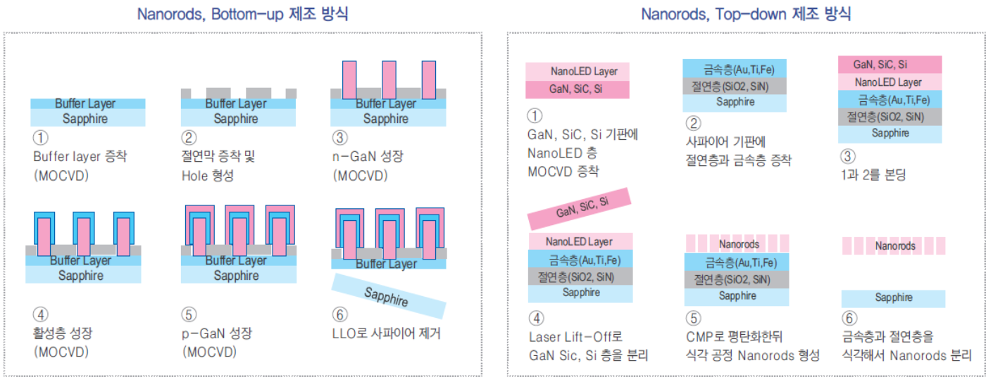
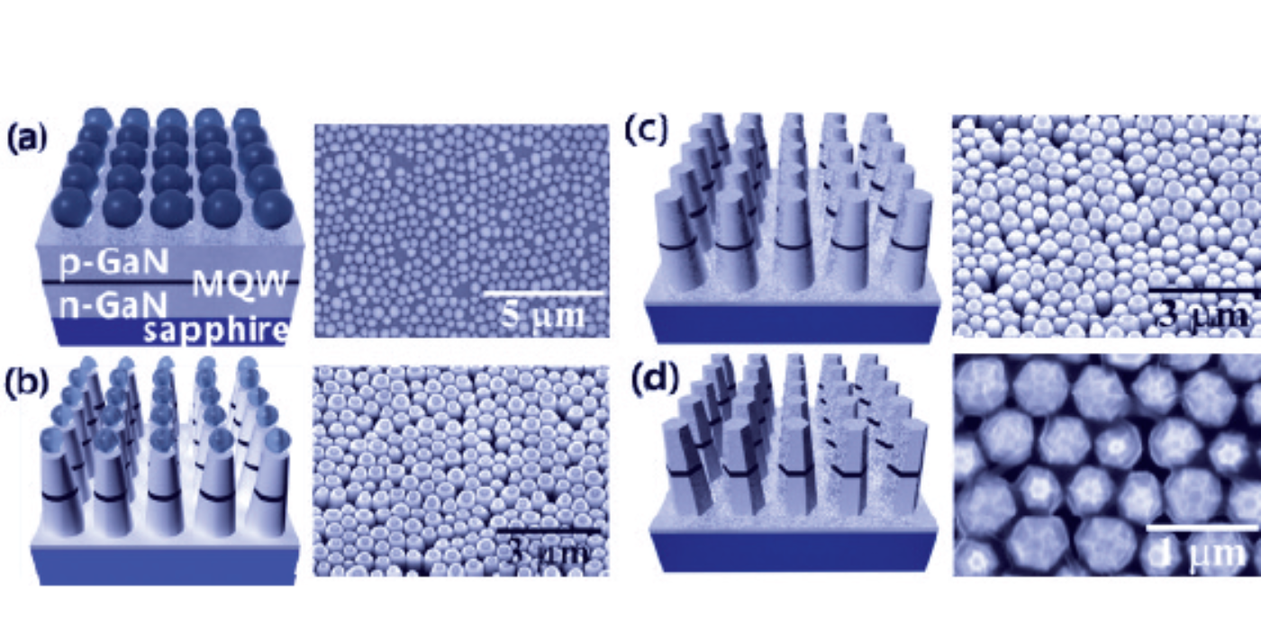
In the top down approach, patterning methods such as etching techniques, are introduced as a low-cost but highly efficient way toward fabrication of high-aspect-ratio 3D GaN micro-/nanostructures. A straightforward method to fabricate GaN nanoLEDs is to etch planar GaN LEDs with nanomasks. The GaN nanorods can be defined by various methods like conventional photolithography, e-beam lithography, and nanoimprint lithography or other low-cost methods, such as SiO2 nanosphere lithography as shown below. Dry etching methods, such as RIE-ICP, can be used to achieve high aspect ratio.
 Hyunik Park, Kwang Hyeon Baik, Jihyun Kim, Fan Ren, and Stephen J. Pearton, “A facile method for highly uniform GaN-based nanorod light-emitting diodes with InGaN/GaN multi-quantum-wells,” Opt. Express 21, 12908-12913 (2013)
Although we don’t know which technique Samsung would follow; for optimized blue emission, the nanorods are said to have a height of 2 um and a diameter of 0.62 um. Exact control of the dimensions over large areas might be a challenge. Further, although the luminous efficiency in theory can be high, it remains to be proven in the fully assembled device. Aggregation effects, size, shape and strain variation in these nanorods can impact the efficiency, color or both.
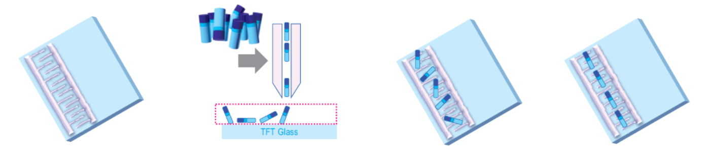
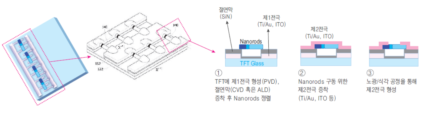
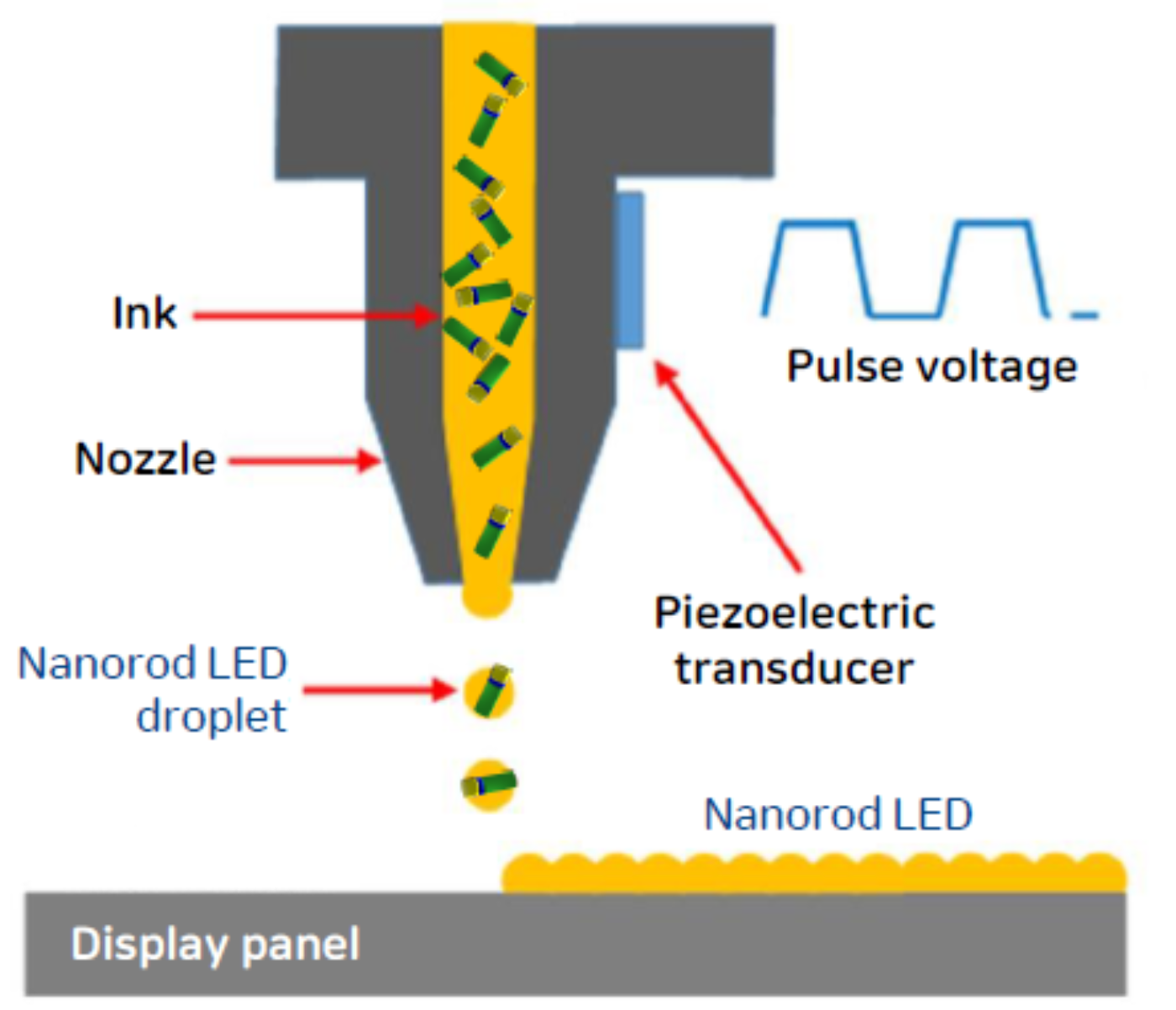
b) Nanorods integration: The nanorods are then integrated onto the backplane to form the device. Inkjet printing technique is currently selected as the means of deposition of the Nanorods. Since the dimensions of the Nanorods are small and this could result in random orientation of the nanorods, first, an electrode is formed on the TFT, for the purpose of alignment with an electric field. The exact process is still not well understood but the sequence of the steps for the integration is as listed below:
 Source: KTB Securities and Samsung Patent
I. First electrode formation on the TFT and insulation layer deposition: Achieved by depositing ITO, Al, Ti, Au, etc. by PVD and patterning by wet etch. An insulation layer is subsequently deposited over the first layer. The insulation layer maybe a SiNXor SiO2 material deposited by CVD or ALD equipment.
II. Inkjet Printing of Nanorods: The nanorods dispersed in a solvent are then inkjet-printed onto the described layer. Currently, we expect this to be a blanket coating on the substrate since pixel level color definition is not required for the blue nanorods. Potential challenges with inkjet methods include clogging of printheads due to micron sized dimensions of the nanorods, poor dispersion of the nanorods in the solvent of choice, inkjet stability and uniform drying of the solvent over large area glass sheets etc. Having a larger diameter nozzle may help some of these problems, but we still believe this could be a challenge.
III. Nanorods Alignment: Nanorods are then aligned by applying a voltage to the first electrode. It is still unknown as to how this would be achieved and how efficient the alignment process is and if good contacts can be achieved by this process. A Samsung patent showing an aligned Nanorod is shown below.
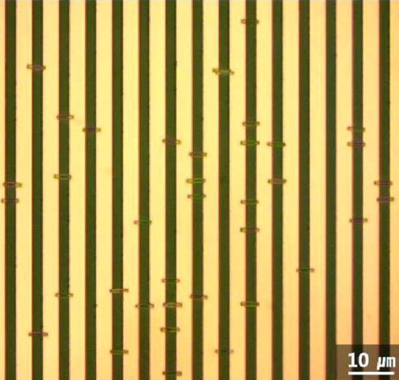 Samsung Patent- WIPO: KR1020190137742
IV) Formation of second electrode for driving nanorods: The second electrode is then deposited by PVD on nanorods. The materials used for this layer are likely to be selected from Ti / Au or ITO. This is subsequently followed by selective etching to define the aperture.
3) Quantum Dot Color Conversion: Since GaN Nanorods emit blue light, we believe there will be no change in color conversion methodology when compared to QD-OLED. The quantum dots will absorb the blue light and down convert it to red or green in the red and green pixels respectively. An additional RGB secondary filter is likely to be used to prevent unintentional excitation of QDs as well to prevent blue leakage due to in-sufficient blue light absorption by Cd-free QDs. The QDCC is expected to be formed by inkjet printing of QDs dispersed along with scattering particles a in solvent free monomer system. The blue pixel will be coated with only scattering particles. A schematic of the process flow is shown below: (SM)