Conventional optical components typically derive light manipulating capabilities from their shape and/or material composition. On the other hand, there are optical components that can manipulate light based on an entirely different approach. This approach is based on so-called metasurfaces. Such components are also able to modify the polarization, phase or amplitude of visible light but do so through the use of a planar, ultrathin, nanopatterend surface.

The use of metasurface based components would seem to be an attractive option for use in a variety of optical system applications. This due to the fact that they offer ultrathin alternatives to a wide range of common optical components including bulky refractive optics and waveplates. Up to now, however, the fabrication of metasurfaces has often included the use of processing steps that can be expensive, time consuming, complex or potentially hazardous. This has prevented broad commercialization of metasurface-based components.
To address these issues, a team of researchers headed by Daniel Andrén within the Physics Department at Chalmers University of Technology (Gothenburg, Sweden) is developing a new approach to producing metasurfaces.
A recent article on this topic by the researchers is entitled “Large-Scale Metasurfaces Made by an Exposed Resist.” It was published in ACS Photonics 2020, 7, 4, 885–892. A copy of the article is available on-line and can be found here.
The approach investigated by the researchers can be explained by paraphrasing this article. The process starts with the use of a standard, off-the-shelf negative resist material such as that widely used in the manufacture of semiconductors. The polymer resist material is spin-coated onto a glass plate. It is then patterned with a single electron beam lithography exposure, to create the required high aspect ratio nanofin structures on the surface. When properly patterned, the resist material can form the metasurface itself, limiting the manufacturing process to essentially a single lithography step. By this means, the time and cost required for processing as well as any associated safety hazards can all be dramatically reduced.
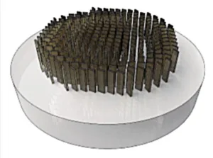
As a proof-of-principle for the technology, the team prototyped the flat optical equivalent of spherical lenses. Full details on the equipment, materials and processes used to fabricate the prototypes are discussed in the article. The prototypes demonstrated both narrow focusing and high resolution imaging. More specifically, the researchers created macroscopic 1 centimeter diameter positive lenses, consisting of more than 600 million individual nanoscale elements. (The researchers made special note of the fact that it was possible to fabricate the prototype lenses during a single afternoon of lab work.) A generic illustration of a lens is presented in the figure below.
Generic image of a metasurface based lens.
The prototype was tested and found to produce an image that displayed even the finest details of the target – just as would a normal camera lens, but with an optic that was thousands of times thinner. Other tests demonstrated that the metasurface was efficient, having a polarization conversion efficiency greater than 50% as well as having the ability to function across the entire visible wavelength spectrum.
The team also prototyped both gratings that exhibited anomalous reflection and metasurface-based cylindrical lenses. In addition, various types of substrates were chosen for use in the prototypes. The point was to demonstrate that the manufacturing approach was compatible with both flexible plastic and metallic mirror substrates.
Reliability testing demonstrated that the metasurfaces were stable over time and could be left in ambient conditions without any noticeable degradation for at least six months. Regarding stability, polymer metasurfaces were demonstrated to withstand temperature at least as high as 100 °C. The metasurfaces did not show any apparent reduction in performance when exposed to the relatively high light intensity of 5 W/cm2 generated by a 532 nm continuous laser source.
In looking to future work, the researchers comment in their article that even faster writing speed could be achieved with other resists that are up to 100 times more sensitive (such as the UV?N series). The researchers conclude with the speculation that their approach could eventually facilitate flat optical components becoming a substantial competitor to bulk optics. Possible applications in display technologies include their use in projectors and miniLED backlights. -Arthur Berman