MicroLED displays are the new technology on the block. And with a new technology, all of the previous givens are being re-examined, including whether the display will be driven with a TFT backplane or with some sort of distributed silicon solution. The aim of this short article is to talk about my overall thoughts on the TFT driving part of the equation.

MicroLED specific requirements
When we are talking about MicroLED displays we are typically talking about displays that have inorganic emitters smaller than 50 ?m x 50 ?m, though in reality we need to be discussing emitters smaller than 10 ?m x 10 ?m for them to be used cost effectively in mainstream displays such as TVs and smaller than this for smartphones. At these sizes, maintaining efficiency is a very big challenge as the small dies suffer from all sorts of non-radiative side-wall effects and as they get smaller the peak current density they need to operate without droop and colour shift increases. The accuracy of how that peak current is delivered is also very important as otherwise the efficiency moves away from peak and the colour may shift.
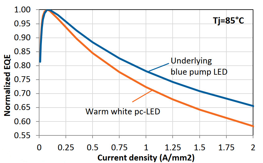 Typical Gan LED Droop means a drop in EQE after the peak current density. Image:Lumileds
So far, CMOS LTPS has been used in nearly all demonstrators as the backplane of choice. This is due to the high current capability of CMOS LTPS and the high speed switching capability. There is still much discussion on how best to drive a MicroLED display, but PWM (Pulse Width Modulation or time-based dithering) schemes have been suggested with very short pulses down to the ns regime in length to achieve good grey-scales. The uniformity of the current driven is important as we have stressed. Moreover, we need to allow for the TFT level computing to generate grey scale using PWM.
The idea of CMOS LTPS in the TV market (as indeed large TVs such as “The Wall”) seems like a contradiction: why would anyone want to use LTPS in a large panel? Over time it is my belief that if the stability and mobility of oxide can be increased and the peak current capacity, then large panels, at least, will adopt IGZO as the active-matrix backplane technology.
Many of the active-matrix MicroLED papers at DisplayWeek 2020 were focused on demonstrating the core technology and used a simple 2T1C circuit. This is the simplest option. By this year, most of the papers are looking at more complex compensated circuits. It seems that while simplicity is always valued, the industry is trying to decide what driving approach and how much compensation is actually needed to get MicroLED to deliver high brightness, colour controlled, high grey-scale images.
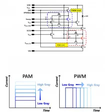
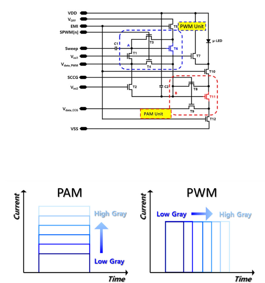
The industry seems to have moved down the path of multi-transistor compensated circuits as part of a PWM approach to TFT-driven MicroLED driving. One example of this was presented by Samsung and Sungkyunkwan University at DisplayWeek 2020. Their paper, as well as a follow up paper from DisplayWeek 2021, demonstrate 9T3C and 12T2C circuits (see first figure for example of 12T2C circuit) capable of Pulse Amplitude Modulation (PAM) and Pulse Width Modulation (PWM) for driving the MicroLED (see second figure for an example of PAM vs. PWM as shown in the referenced papers).
This, then, is a circuit at the complex end of the scale where both amplitude (and hence constant current) and pulse width are both independently controllable. I imagine that in the coming years, players will experiment between the two extremes, to achieve the goal of controllable (fixed, stable amplitude) high current, very fast pulses.
 Figures adapted from Y.-H. Hong, E. K. Jung, S. Hong, and Y.-S. Kim, “61?2: A Novel Micro?LED Pixel Circuit Using n?type LTPS TFT with Pulse Width Modulation Driving,” SID Symposium Digest of Technical Papers, vol. 52, no. 1, pp. 868–871, May 2021, doi: 10.1002/sdtp.14822.
Another Thought
And I have one more thought to add to this. The requirements of MicroLED driving are found from fast switching transistors or diodes, with high current draw capability due to decent mobility. One of my clients, Amorphyx, has two TFT alternative solutions that get to these requirements – the AMeTFT high mobility oxide transistor and their very fast switching AMNR approach. The aim overall is to use diodes and higher performance transistors to reduce the complexity of the overall design down from this 12T2C type levels.
Their first circuit, the 211 circuit (and concept overall) uses two AMNR voltage controllers plus a very stable, high current, high mobility oxide transistor, may be able to provide accurate current densities and at short pulse times without the need much more complex circuits. The AMNR voltage divider can be used explicitly for some of the Vth compensation and the fast oxide AMeTFT (Amorphous metal) transistor with high stability and mobility can enable shorter pulses.
Today’s industry is facing a number of driving challenges: “TFT or Micro IC?” being the first fundamental question. “Oxide or LTPS?” becomes a second. And then fundamentally the industry needs to deliver high current density peaks in very fast pulses. Samsung’s paper shows the theoretical ‘all singing, all dancing’ LTPS-based circuit but no-one will want to put that into production*: the industry will experiment to find simpler solutions. – Ian Hendy
* That would mean nearly 300 million transistors for a 4K display, 1.2 billion for an 8K! Editor.
Ian Hendy is a Display Strategy Consultant based in London, UK. Hendy Consulting provides growth strategy, technology strategy and deal/M&A assessments for players throughout the display value chain. Mattrix is a client of Hendy Consulting.
This article was moved out from behind the Display Daily paywall by Amorphyx, so does not count towards your free allocation of articles.