It’s sometimes hard as an independent analyst to work out whether a claimed technical breakthrough is really what it seems. I don’t have a team of engineers and scientists on the payroll to evaluate the technology, and given the very wide range we cover, I’d have to be a global tech giant to really evaluate someone’s ideas. So it’s really pleasing when you see a global tech giant investing in the technology.

Now the technology in question is from iBeam, which claims to have a breakthrough technology for microLED displays and we have been reporting their technology for a couple of years. It was intriguing and looked credible, but now it has had two rounds of investment from Samsung Ventures and that company has a seat on the board. That makes the technology much more likely to be real! (although it’s no guarantee – see Magic Leap!)
(Coincidentally, last week I wrote about OTI Lumionics and literally two minutes before the article was published, I got a release saying that LG Technology Ventures was investing in the firm. That made that story more credible, too! Materials Remain Important for Under-Display Cameras and OTI Lumionics Announces Strategic Investment from LG Technology Ventures).
Vladmir Matias is founder and President of iBeam Materials of Santa Fe and he spoke at the DSCC/SID Business Conference during Display Week. Nearly two years ago, Chris wrote a DD about the firm, but this was the first time I had heard a talk. (iBeam Materials Working on GaN-on-Metal Process for LEDs)
The firm was spun out of Los Alamos Laboratory in 2011 and is a world leader, Matias said, in ion beam crystal alignment used in superconducting wire, and that technology is exploited in a range of applications.
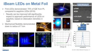
He started by highlighting the potential advantages of microLED displays, which we’ve covered many times. Everyone knows they will be great, but nobody really knows when they can be made in high volume at a low enough cost for the mass market. iBeam wants to monolithically integrate LEDs, transistors and sensors into a single sheet. To do this, you would like to be able to use GAN epitaxy (epi) processes (which are used to make LEDs) over large areas and at low costs, but today GaN LEDs are made on 6″ sapphire wafers and the epi cost alone is around $2-$3 per sq cm (which would make a smartphone display around $250, so not competitive).
However, iBeam says that it can make LEDs directly on polycrystalline metal foil (without transfer) using an iBeam planarisation layer and crystal aligned layers to replace the sapphire substrates. The process is called Ganox and epi-GaN layers are fabricated on single crystal-like layers that have been deposited on polycrystalline or amorphous substrates. Ganox can also be used with glass or ceramic substrates as long as they are compatible with the GaN deposition process.
GaN devices could even be made on a roll-to-roll basis which is quite different from other processes that need transfer of the LEDs from the semiconductor processing to the display. Only by depositing directly on the substrate can you scale to a large enough area and get the dramatic cost reductions needed, Matias said. The Ganox process also allows large scale integration of LEDs, in the same way that LSIs were created by scaling a basic process and, Ganox could do the same for photonics, he continued. With this scaling new classes of products are likely to emerge.
iBeam worked on an ARPA-E project with Sandia National Labs and demonstrated microLEDs on a flexible metal substrate in 2018 and GaN FETs on metal foil in 2019.
The Next Step
The next step is to develop high output and low cost materials. The Ganox ‘secret sauce’ is in the ion beam crystal alignment process which enables it to deposit a single-crystal like layer on (any) smooth substrate. Depositing materials using conventional techniques on an amorphous or polycrystalline layer usually resuts in grains being randomly aligned. However if the deposition is subjected to an ion beam at an angle (and under certain conditions), the grains can be aligned. The process is very fast – a 5nm layer can be deposited in one second making it high throughput at low cost. It allows the epi-GaN process on the treated substrate.
In 2018, the firm demonstrated 70% IQE compared to sapphire LEDs but more can be done to improve efficiency, especially by improving the light extraction efficiency and iBeam can ‘approach the performance of sapphire’ eventually. Mechanical flexibility of its materials is down to 7mm radius.
 Click for higher resolution
The firm has also made transistors on metal foil using Ganox so large area displays can be made using the transistors to control the LEDs, with no transfer of the microLEDs or transistors. QDs can be used for downconversion to red and green. There is plenty of room for extra LEDs for redundancy or for extra circuitry, Matias said.
Unique features is that scaling of the cost goes with the area (like LCD), not with the pixel count (like traditional LEDs). That means that high resolution has little extra cost and the technology could be important for light field displays that need huge numbers of pixels. The LED size is not limited, so you can pick the size to optimise for the efficiency and application. Sensors can also be integrated.
The technology has a relatively low capex, with a $100 million roll-to-roll facility in contrast to a $1 billion wafer reactor or a $2 billion to $3 billion LCD fab and this kind of fab could be built outside Asia. A small footprint means lower operating expenses. Matias said that it is aiming for a >20X reduction in epi Cost down to <$0.10 per sq cm, which would be competitive with OLEDs, but with better performance.
The firm expects future displays in 3D and bigger displays and Ganox can meet this target and be truly disruptive to the industry. Hence, I guess, the Samsung Venture investment! (BR)