Display Daily is a media sponsor for the Techblick Mini- and Micro-LED and Quantum Dot events on 30th November and 1st December. The firm has kindly provided us with a number of interesting extracts from some of the talks that will be give at the event and we have put them in two articles – one today and one on Thursday of this week (we will count them as one if you have a free registration).

In this article, using select technology slides, we highlight several interesting advancements in MicroLED and/or QD displays. More specifically, we cover 3600PPI “Silicon” Displays | Gravure printed microbumps | Electrohydrodynamically printed QD color converters | Laser LLO and Transfer for MicroLEDs | QD vs Phosphors | Energy saving credentials of microLED
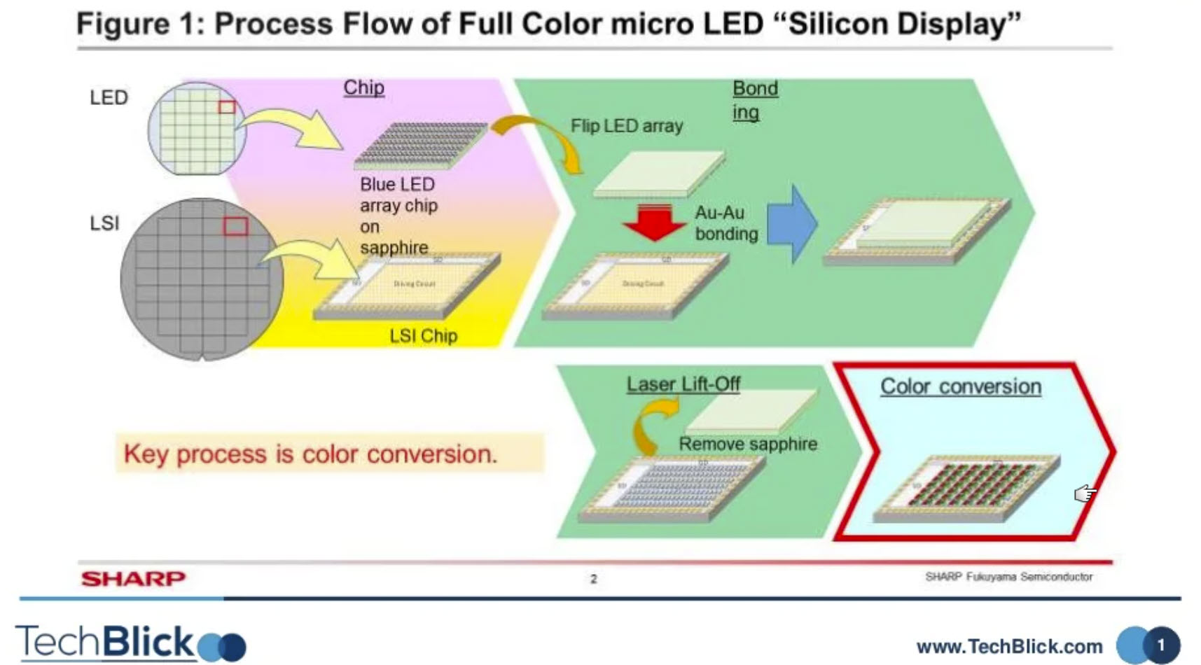
“Silicon” Displays with an incredible 3600ppifull color using microLED and QD technology?
As shown in the slide below, first blue-only ?LEDs are formed on a sapphire substrate. Here, one LED array contains 352 x 198 microLED dies of 24 ?m x 8 ?m in size. In parallel, an LSI chip containing the driving circuitry is formed on a silicon wafer. Here, the cathode (N-type electrode) and anode (P-type electrode) are fabricated for each microLED die to apply driving voltage independently to each die. The Au bump electrodes are fabricated in accordance with the pitch of the LED dies. The two substrates are flip-chip bonded using Au-Au bonding.
Here one can already see the parallel to the silicon and optoelectronic industry (vs. the traditional thin film display industry!). Next, the sapphire layer is removed via laser lift off. Finally, Cd-free quantum dots (green and red) are deposited atop the microLED dies to enable R G color conversion. This way one achieves RGB colors
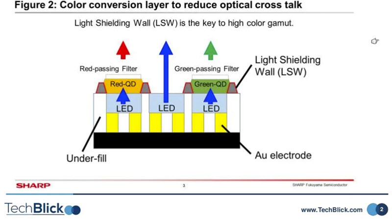
The device architecture is shown in slide 2- here one can see the location of GaN uLED dies, Au bumps, as well as light shielding walls and quantum dots (QDs). This way, a full color 1,053 ppi display is formed.
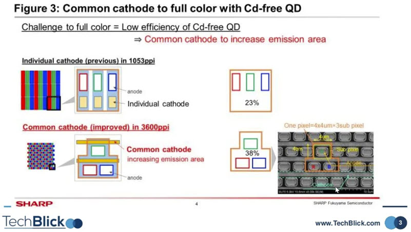
However, given the small size of the emissive area of uLEDs, the brightness is low. An innovative solution here is to switch from individual driving cathode electrodes to a common one, thus freeing up more spaces for uLEDs. As shown in slide three, the light emission in one pixel was improved from 23% to 38%. As a result, brightness of 11k cd/m² was achieved. This is an excellent progress. Of course, it is not the final game as even at 11k cd/m² the brightness is not yet not sufficient for outdoor AR applications.
Gravure Printed Microbumps for MicroLEDs
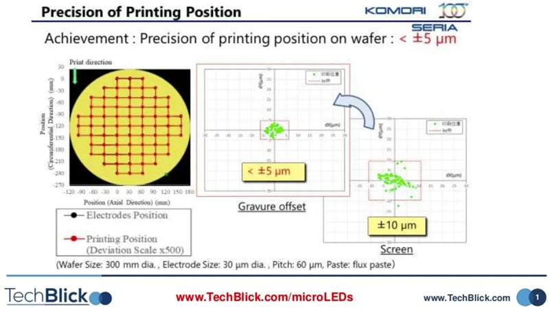
As microLEDs inevitably shrink in size, the micro-bumping requirements for the microLED dies becomes more challenging. Direct wafer-based printing based on gravure offset techniques offers a promising solution in this regard. Indeed, this is another field where printed electronics can play a role.
As seen in the slides below, gravure printing can print microbumps printed using flux paste, achieving a printing precision of 5 µm within a range of 300mm. The first slides show the precision of the printing position on a wafer. In particular, it compares it with screen printing, showing how gravure printing advances the fine feature printing capability w.r.t screen printing (+/-10 µm although screen printing too can and will also advance)
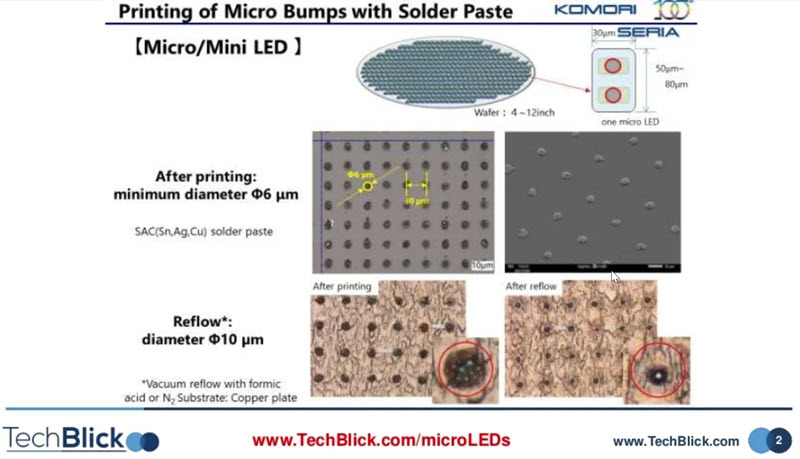
As shown in slide two, the minimum diameter that can be printed with SAC (Sn, Ag, Cu) solder paste is 6 ?m and the distance between the centers of the bumps is 30 ?m. Reflow has been successful with a minimum diameter of 10 µm. This way for example, a microLED die in the size of 30µm by 50 or 80µm can be supported.
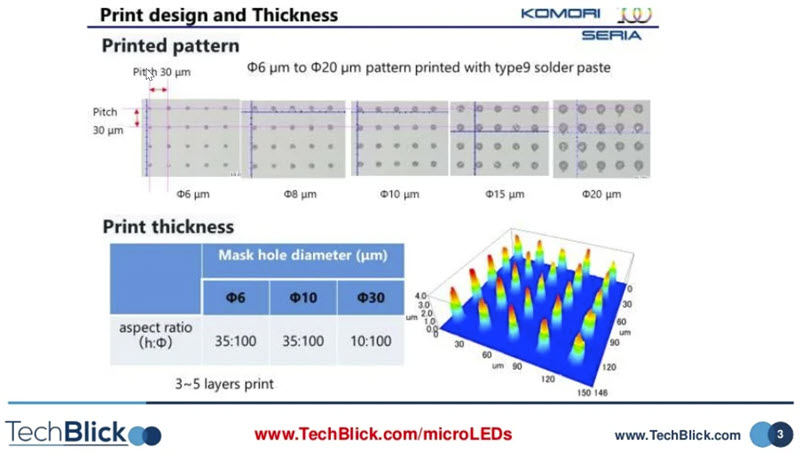
Furthermore, as shown in slide three, this technique also offers the possibility to control the thickness by printing several diameters. The smaller the bump diameter, the higher the aspect ratio.
These are very nice results, showing the viability of gravure printing technique for microbumps. This technology can support current and near-term generations of microLEDs but will it evolve as microLED dies further shrink in the longer term?
High-PPI RGB microLEDs, printed electronics, and quantum dots?
The three themes are closely linked since QDs can be digitally printed as color conversation materials atop blue microLEDs to enable wide color gamut RGB microLED displays without requiring a separate transfer step for each color.
Inkjet is the common technology investigated for such a purpose. As shown below by Prof.Armin Wedel, however, its 4pL droplet is too large, allowing at best a 40?m pixel and not able to reach even 850 dpi
Electrohydrodynamic printing (EHD) can however address this issue. In EHD, the droplets are pulled out by an electric field from a nozzle which sits close (50?m or so) to the surface and thus requires a good printing facility.
As shown below, the droplet volume is only 0.5pL, enabling 1-10?m pixels in the lab and 15?m reproducibly. This will enable one to achieve 850ppi and 1000ppi!
Slide 2 shows an example of a QD color filter (QD-CF) for a microLED display deposited using EHDJet. Here, 15?m pitch is reported, achieving 1000ppi. The roadmap will be to evolve the technology towards even 2000ppi!
These are excellent advancements of the art and technology, paving the way for the development of high-PPI microLED technology
Of course, EHDJet is a relatively new technology. It is mainly single head and slow, although multi-head print heads are emerging. Nonetheless, it is an elegant solution for depositing color filters on high-PPI microLED displays.
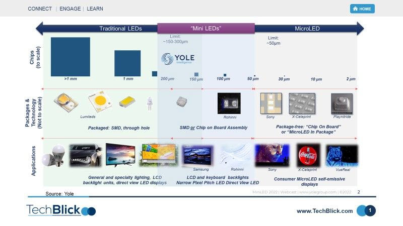
How are micro-, mini-, and traditional LEDs defined?
Eric Virey – super analyst in the field and from the Yole Group – prepared the below chart, showing the key differences between each.
Traditional LEDs come in SMD or through-hole packages and the dies are typically 1mm or larger. This well-established application finds use in general lighting, automotive lighting, and LCD backlights.
MiniLEDs are typically smaller than 200?m in die size but larger than 50?m, and come in SMD or CoB (chip-on-board) packages. They are currently commercial and find applications in LCD and keyboard backlights, narrow-pixel pitch LED direct view LEDs, and other sectors. In the LCD sector, they are suited to provide local dimming to improve contrast, making LCDs more like OLEDs on this feature.
MicroLEDs are very small, typically smaller than 50?m. The size of the microLEDs is expected to shrink further as the technology progresses to reduce LED cost (more LEDs per wafer) and transfer cost/time (e.g., more LEDs transferred within the same stamp).
Evidently each class of LEDs is very different in every sense from growth techniques to performance to application.
You can hear more about all of these topics at Techblick’s first-ever specialist microLED and QD event. (KH)