The development of microLED based displays has driven the need for a high yield, cost effective means of microLED mass transfer. At this time, however, conventional transfer technologies can fairly be described as needing improvements in transfer yield as well as rotational and translational transfer accuracy. Also desired are improvements in compatibility with the subsequent bonding processes.

A team of researchers from Guangdong Institute of Semiconductor Industrial Technology, the University of Tokyo and Foshan Debao Display Technology Co Ltd. (Foshan, China) are attempting to address these issues by developing a method that allows fast, effective, wafer level transfer of microLEDs.
A recent publication by the team on this subject was entitled “Wafer-Scale Micro-LEDs Transferred onto an Adhesive Film for Planar and Flexible Displays.” The article was published on-line in Advanced Materials Technologies. A copy of the article is available for purchase here.
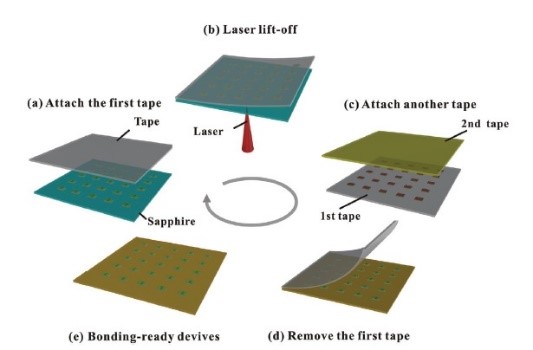
In this study, the researchers refer to their new process as Tape Assisted Laser Transfer (TALT). The TALT process can be explained with reference to the graphic below.
Outline of the steps in the TALT process for wafer level microLED transfer.
Drawing upon the explanation presented in the article, the process steps in the graphic are as follows:
- An adhesive tape is laminated to the array of microLEDs formed on a sapphire substrate.
- The sapphire substrate is then removed using laser lift-off. The optimized laser spot was 30 microns in diameter, the optimum pulse width was about 10 ns and the optimum laser power was about 5.5 mW. The result of the laser lift-off process was the wafer scale release of the microLED array to the first adhesive tape.
- Previous to flip-chip bonding of the microLEDs to a driver board, the microLEDs must be turned upside down. This is achieved by attaching a second tape to the microLED array in which the adhesion of the second tape is stronger than that of the first tape.
- Due to it having stronger adhesion, the microLED array is released to the second tape by simply peeling away the first tape.
- At this point, the thin film microLED array is ready for transfer and subsequent use in a flip-chip bonding process.
The results of both optical and electrical tests fully described in the article indicated that microLED device performance experienced little degradation when values measured before transfer were compared to values measured after transfer. In addition, the new transfer method demonstrated fast, wafer level microLED transfer with extremely high yield of about 99.8%* and highly accurate transfer displacement with an accuracy of less than 0.5 µm. Another feature of the approach is that, combined with a shadow mask, the laser lift?off process can enable the selective transfer of microLEDs to the tape. A final feature of the approach is that the transferred thin film microLEDs are well suited for use with a subsequent “bumpless” bonding process when low melting point solder is used. The researchers believe that their new approach can be scaled up to transfer microLEDs fabricated on even larger size wafers.
The article reports that prototype devices including both planar and deformable display were developed by the researchers. Based on these results, the researchers went on to suggest that the new method is promising for fabricating high resolution microdisplay devices for potential applications in areas such as VR/AR headsets, wearables and mini-projectors. – Arthur Berman
Guangdong Institute of Semiconductor Industrial Technology, Guangdong Academy of Sciences, Zheng Gong, [email protected]
* Although 99.8% as described by the group sounds good, when you are dealing with, for example, even just a FullHD display, that would mean 12,000 defective pixels. That’s one of the reasons that microLED is proving tricky. Editor.