A start-up company out of Cambridge University, Poro Technologies Ltd. (Sawston, United Kingdom) or Porotech has announced the upcoming availability of a native red LED epiwafer product. The development of an efficient native red technology is represented as a key enabler for microLED applications and the associated industry.
This article is based on and partially paraphrases one published in the DSCC Weekly Review subscription newsletter in Vol 3 N48 page 17 published on November 30. The content appeared in an article entitled “Porotech Targets MicroLED Market with Native Red Epiwafers” by Guillaume Chansin.
To start this article, here are a few words of background information.
Conventional blue LEDs are typically manufactured by epitaxial growth of GaN on sapphire wafers and incorporates InGaN/GaN multi-quantum well structures. Increasing the indium content can shift the emission to a longer wavelength. A shift to green is effective however, further shifting to achieve pure red has proven difficult. This is due to the fact that the lattice of the GaN buffer layers is not a good match to the lattice of the InGaN quantum wells. One manifestation of this mismatch is that red emission utilizing InGaN is found to occur at a greatly reduced efficiency.
This loss in efficiency is one reason why commercial red LEDs are mostly based on aluminum indium gallium phosphide (AlInGaP) materials or blue color converted to red. It can be noted, however, that although AlInGaP materials work well in applications that require regular sized LEDs, performance deteriorates as the LED gets smaller. More specifically for microLEDs, which typically measure 100 ?m or less, there is a large efficiency drop due to the large carrier diffusion lengths and high surface recombination velocity. To put this into context, wall plug efficiency is about 10% for blue or green displays but only about 1% for red displays.
In addressing these issues, Porotech has developed a technology in which holes a few tens of nanometers wide are etched inside the GaN layer. Porous GaN of this type can be thought of as semiconductor composite of solid GaN and air. By making the semiconductor porous, it becomes possible to tailor the properties of the material to the needs of specific applications.
Porotech creates the nanoscale porosity in GaN wafers using electrochemical etching. The etching process is “conductivity selective.” That is, the rate at which etching proceeds depends on the extent to which the material has been doped. Substantial etching occurs in doped layers while undoped layers experience little etching thus allowing the formation of complex, porous 3D nanostructures. A further detail describing this process is that the etchant flows into and out of the doped layers via channel-like dislocations. Even in the highest quality GaN wafer there are on the order of 105 such nanometer sized defects per square centimeter.
Porotech has found that, by using this conductivity selective etching mechanism, it is possible to create GaN structures over the entire surface of the wafer. This, in turn, enables an entirely new set of material properties.
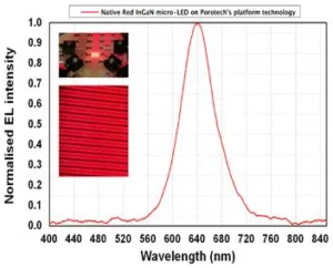
Porotech reports that samples of the company’s native red InGaN microLEDs show improved performance over conventional AlInGaP and color converted red at very small pixel size. The team demonstrated material having an emission wavelength at 640 nm when the current density level was 10 A/cm². The graph in the figure below charts the emission spectrum of a native red microLED that was fabricated utilizing Porotech’s porous GaN technology.
Emission spectrum of a native red microLED fabricated utilizing Porotech’s porous GaN technology.
Porotech has stated that the porous GaN fabrication process technology is compatible with the standards and processes typically in use today by industry to fabricate LEDs. The company believes that this should enable rapid commercialization of porous GaN technology.
The company reports that porous GaN technology has been tested on wafers up to eight inches (200mm) in diameter and is believed compatible with wafers with a diameter of up to 12 inches (300mm). This includes wafers of sapphire, silicon, silicon carbide, GaN and other industrial wafer substrate materials. It can be noted that Porotech currently uses a fabless model and their partner foundry is Enkris Semiconductor.
In an interesting variation of Porotech’s technology, the team has filled the pores in a porous GaN wafer with a halide perovskite to create an optoelectronic material. Using this technology, it may be possible to produce a material in which luminescence degrades more slowly that in conventional materials.
At this time, initial investment funds are being used by the company to transfer the production process from the laboratory to a pilot plant located in Cambridge, UK. The plant is planned to be operational by June. The company has expressed interest in licensing their porous technology. -Arthur Berman