
The structure of Phosphorescent Organic Light Emitting Diodes (PhOLEDs) typically includes multiple layers of various organic materials. Simplifying the structure of the device is an important goal in the ongoing development of PhOLEDs.

One approach to simplification is to create a single layer device. Such a device would consist of only the electrodes and an emissive layer. Unfortunately, removing functional layers from PhOLEDs has been found to drastically decrease device performance.
A team of researchers led by Fabien Lucas of the Ecole Polytechnique, Institut Polytechnique de Paris (Palaiseau, France) have undertaken research to address this issue. The approach adopted by the team is based on a “rational molecular design” of the emissive layer. A recent article on this topic by the team is entitled “Simplified Green-Emitting Single-Layer Phosphorescent Organic Light-Emitting Diodes with an External Quantum Efficiency > 22%.” It was published in Chem. Mater. 2022, 34, 18, 8345-8355. A copy of the article is available for purchase here.
The technical description of the approach adopted by the team is expressed in this article as “The emitting layer of this device is constructed on the barely studied Ir(ppy)2acac phosphor and a high efficiency host material possessing a Donor-spiro-Acceptor design.”
Using this approach, the team reported development of a prototype green light emitting single layer PhOLED that achieved an external quantum efficiency of 22.7 %. This is represented as the highest ever achieved by a single layer PhOLED – and demonstrated that a simplified single layer PhOLED can be almost as efficient as a multi-layer PhOLED.
Included in the article are descriptions of the means used to test the electro optical properties of the prototype devices. Such means included morphological (atomic force microscopy), photophysical (time resolved spectroscopy) and charge transport studies.
In the article, the researchers explain that the high level of performance demonstrated by the green light emitting, single layer PhOLED prototype device can be explained by several factors:
- An excellent balance of the charge carriers within the emissive layer. (The highest occupied molecular orbitals and lowest unoccupied molecular orbitals in the emitter material align with the Fermi levels of the material in the anode and the cathode. This maximizes hole and electron injection respectively.)
- A rapid radiative deactivation process.
- A material that exhibits excellent ambipolarity. (Ambipolarity occurs in materials in which positive and negative charge carriers can both transport concurrently.)
- A surface that is physically smooth
Regarding this last point, the figure below graphically illustrates the surface of the emissive layer. It was made using an atomic force microscope.
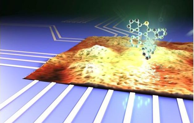 A graphic representation of the surface of an emissive layer.
A second focus of the team’s research was to simplify the approach used to synthesize the emissive layer material used in the single layer PhOLED. The incentive for this effort was to further reduce production cost as well as to reduce the “environmental footprint” of device manufacturing. The details of the approach developed by the team are presented in the article and characterized as short, high yielding and low cost.
The researchers conclude their article by expressing the opinion that “This type of simplified devices appears nowadays as a credible alternative to the well-known multi-layer technology for the future of OLEDs.” – Arthur Berman
University of Rennes, Cyril Poriel, [email protected]