A team of researchers headed by Shoichiro Nakao of the Department of Chemistry within the School of Science at the University of Tokyo (Tokyo, Japan) have demonstrated the highest mobility in a thin film of tin dioxide ever achieved. The improved mobility not only enhances the conductivity but also the transparency of a thin film of the material.

A recent article on this topic by the team is entitled “High mobility approaching the intrinsic limit in Ta-doped SnO2 films epitaxially grown on TiO2 (001) substrates.” It was published in Scientific Reports, 2020; 10. A copy of the article is available on-line and can be found here.
In their article, the researchers define the challenge in this work by explaining that
“Generally, transparency and conductivity cannot coexist in a material. Typical transparent materials such as glass or plastic are insulating, whereas conducting materials like metals are opaque. Few materials exhibit transparent conductivity.”
The material that was the subject of this investigation by the team was tin dioxide. SnO2 can be made into a semiconductor however, up to now, high mobility in SnO2 has been found only in bulk crystals, not thin films. A key parameter describing semiconductor performance is the Hall mobility (?H) which is a measure of the mobility of the electrons. A high ?H is desirable. Unfortunately, ?H is found to be somewhat low even in thin films of SnO2 in which the epitaxial growth process has been optimized. Low electron mobility in SnO2 has limited practical applications for the material.
The low value of ?H in epitaxially grown SnO2 thin films is primarily attributable to the fact that the lattice of the SnO2 is not a good match to the lattice of the substrate on which the thin film is grown. A second important factor that effects ?H is carrier density (ne). Unfortunately, the changes in ?H that result from variations in ne are complicated. On the one hand, an increase in ne enhances the screening of the Coulomb scattering potential and thus increases ?H. On the other hand, one means to increase ne is to increase the concentration of dopants but this decreases ?H due to impurity scattering.
Based on these considerations, the current research focused on developing means to increase ?H in epitaxially grown thin films of SnO2 by improving the match between the lattice of the SnO2 thin film and the lattice of the substrate.
The approach investigated by the researchers in their effort to produce an improved material centered less on the materials themselves and more on the means used to produce the thin film. More specifically, a highly focused laser was used to evaporate pellets of pure tin dioxide resulting in the deposition and growth of a thin film of the material on a substrate. Using this process allowed the researchers to explore different growth conditions as well as means to incorporate dopants.
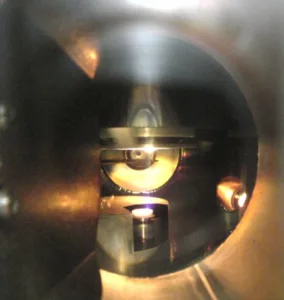
A detail of the equipment used to create the thin films of SnO2 is illustrated in the photo below.
Detail of the equipment used to deposit thin films of tin dioxide.
Using this approach and in a series of experiments, the researchers investigated the transport properties of SnO2 thin films that were lightly doped with tantalum and epitaxially grown by pulsed laser deposition on titanium dioxide (001) substrates. The TiO2 (001) substrate is isostructural to SnO2. That is, there was only a small mismatch between the lattice of the thin film and the lattice of the substrate.
(Note that (001) are Miller Indices. “These are a symbolic vector representation for the orientation of an atomic plane in a crystal lattice and are defined as the reciprocals of the fractional intercepts which the plane makes with the crystallographic axes.” Also note that isostructural means “relating to or having a similar crystal structure in that the atoms correspond in position and function although there may not be close chemical relationship.”)
The article contains a great deal of detailed information on the means of forming the thin films, measuring the properties of the thin films and the results of these measurements. Bottom line in the report is the finding that an increase in ne by tantalum doping dramatically enhanced ?H, probably owing to a screening of the carrier scattering by the grain boundaries and dislocations.
The researchers conclude their article with the observation that potential applications for improved thin film SiO2 include next generation LED lights, photovoltaic solar panels and touch-sensitive display technologies. -Arthur Berman
University of Tokyo, Shoichiro Nakao, [email protected]