This is the second part of a summary of developments in the use of printing in display manufacture, which will be explored in more depth at the “nnovations & Market Trends In Displays & Lighting” virtual event in July. Part 1 is here (The diverse world of printing in displays: how printing impacts AMOLED, AMQLED, microLEDs,AR/VR and beyond – Part 1)

MicroLEDs: printed in every step of the process from wafer onwards
MicroLEDs remain a topic of intense interest in the industry. I want to showcase how printing and R2R can deliver value here.
One of the main challenge in microLED fabrication is to develop a high-yield (>>99.99%) and high-throughput transfer process. Many approaches have been tried. Several interesting techniques involve some form of printing (stamp transfer, R2R, etc). Here, I only highlight two interesting approaches.
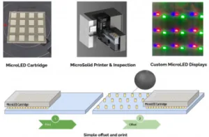
The first is from VueReal which is developing a cartridge-based approach. The process is shown below. Here, the donor substrate containing the microchips is brought into contact with the receiver substrate. The two substrates are then aligned before the transfer takes place. There is a need to apply some force mechanism to overcome the force keeping the microchips attached to the donor substrates. It is not clear whether this is mechanical, heat adhesive (based on material added to receiving substrate), or a combination thereof.
 Schematic outline of the process steps involved in VueReal’s cartridge-based printed microLED approach. To learn more see here
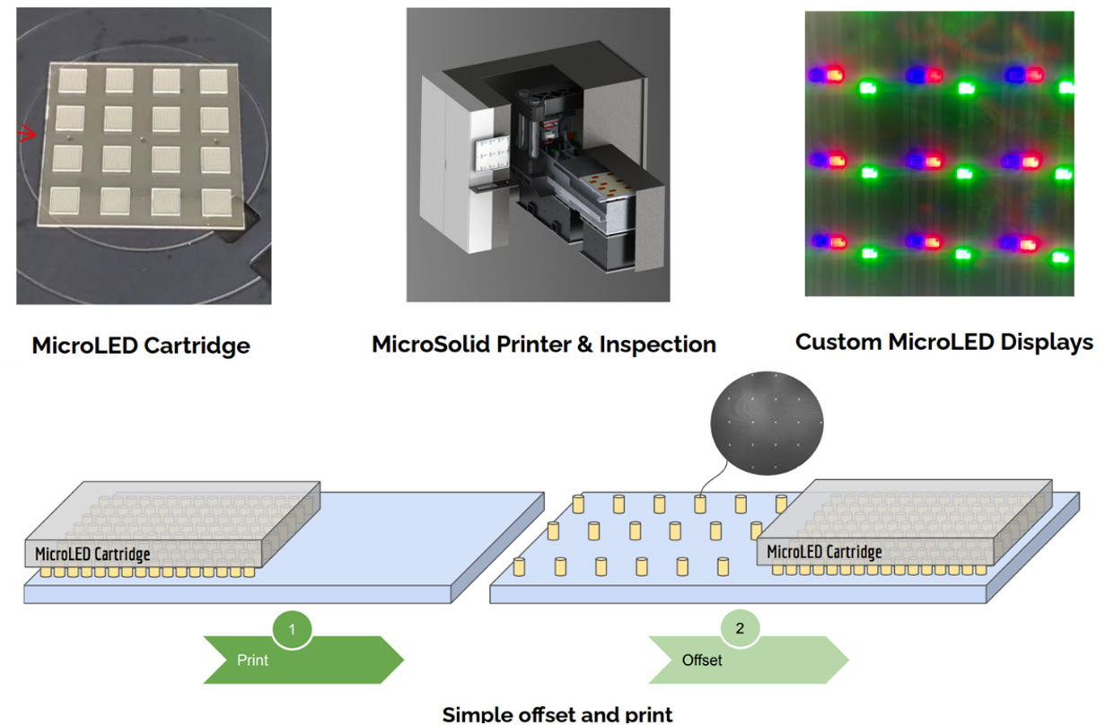
Another interesting, earlier stage, development is by Parc, a Xerox company. The idea is based upon xerographic printing. Here, micro chips such as GaN microLEDs are suspended in a solution. They are then cast onto an active-matrix substrate controlling a 2D array of electrodes which generate electrostatic force to spatially move the individual chips under the gaze of a camera. The assembled microchips are then transferred using a roller onto the final target substrate.
The 2021 demonstrator is still small size (2.5 x 2.5 cm) on 50?m LEDs with no yield data. The assembly process is achieved using a projector addressing a photoswitch array. The assembly process- from mass disordered deposition from liquid to final alignment- is shown below. Currently it is too slow, but an order of magnitude improvement can make it competitive.
The process has interesting development potential as it does not require any special microchip structure. The alignment and positioning is also software controlled, thus allowing arbitrary and complex shapes.
The transfer step has been receiving substantial attention in recent years. There are many other critical steps in microLED production too. I mention this because printing and conductive inks can play important roles in some of these steps too.
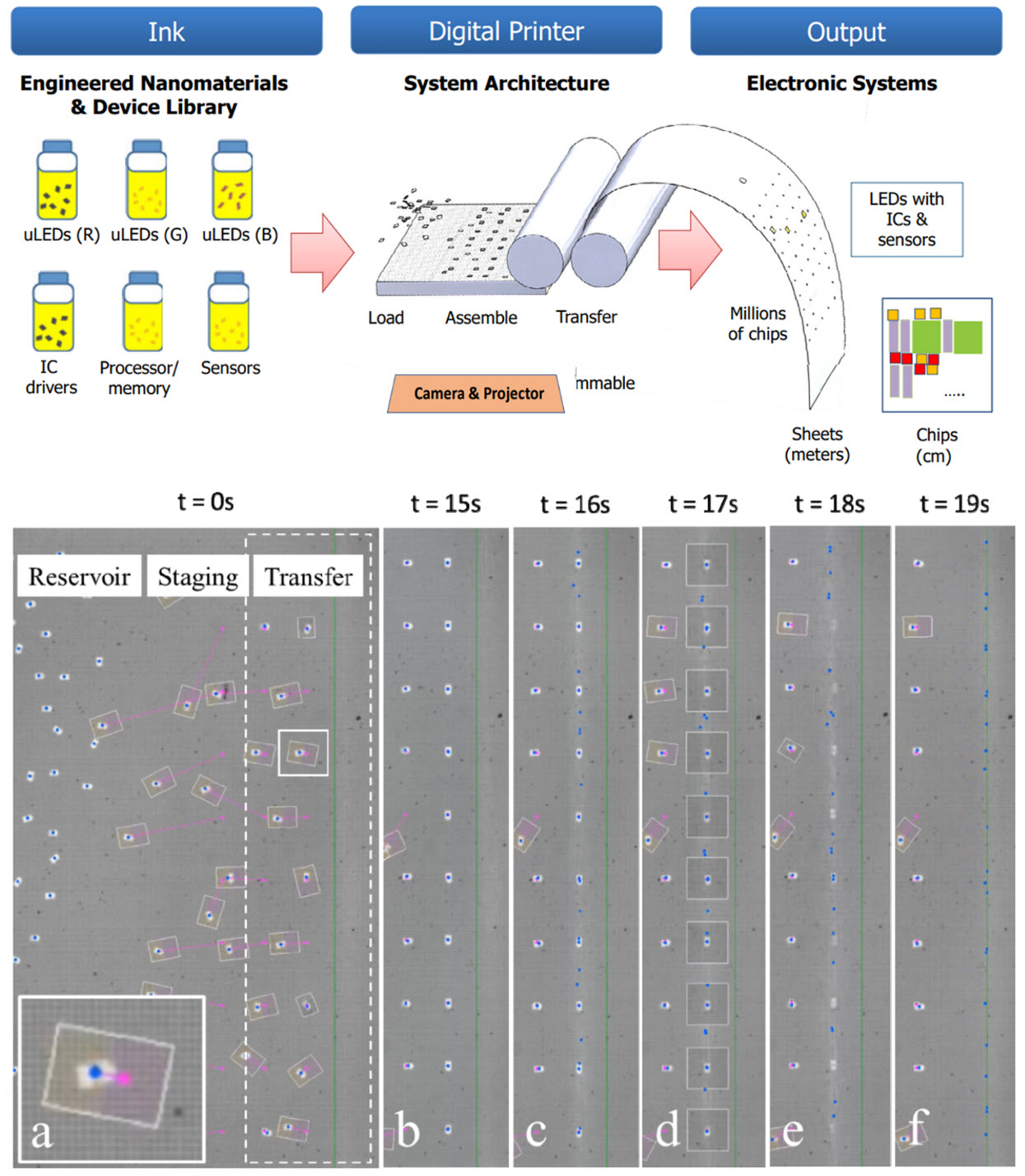
The image below, by Applied Materials, shows various examples. Screen printing can be used to print conductive pastes to fill vias. It can be used to print fine-line electrodes between the front and backplanes. Furthermore, it can also print wrap-around electrodes, connecting the microLEDs with the driver IC. Finally, it can print various adhesives (solder, ECA, etc) for the placement and bonding of micro LEDs.
 The above images are from Applied Materials. They show how advanced fine-line screen printing can play a role in microLED fabrication. Screen printing can, without requiring a vacuum-based PVD process and etching, print fine-line electrodes and interconnects, create wrap-around electronics, fill vias, and even place attach materials. To learn more see here
There are many incredible innovations in the microLED field. Another one that we wish to highlight is in creating a method to assemble large-area microLED displays from tape-on-reel approach.
This is shown below. Here, the microLEDs are first transferred into a larger panel and are then cut into smaller tiles. The tiles undergo an inspection step and the black filling material is added to enhance contrast. The titles are then added onto a reel, creating a tape-on-reel approach enabling the construction of large microLED displays using a SMT-like process! This is a very interesting innovation in the field by PlayNitride.
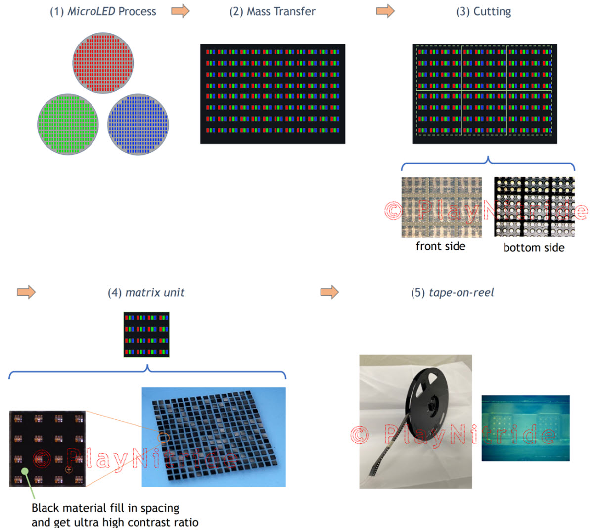 These images show the steps needed to create a reel-on-tape approach to making large-area microLED displays. This innovation is by PlayNitride. To learn more see here
Waveguides for AR/VR displays
There are many other uses of printing or R2R/R2P in the display industry. Another use case is in R2P (roll-to-plate) nanoimprinting for creating in- and out-coupling features for AV/VR glasses. Such in- or out-couplings can be made on 300mm wafers, but the throughput is low. With R2P nanoimprinting the throughput may be substantially extended.
An interesting approach is by Morphotonics. Here, they tile together their nanoimprint stamps to create a Gen 5 R2P nanoimprinting line able to achieve sub-micron features and 480 eyepieces per imprint cycle. The R2P nanoimprint process requires solvent-free resins with high refractive index. Here, for example, zirconia and titania based formulations by Pixelligent can result in resin with a refractive index of 1.857.
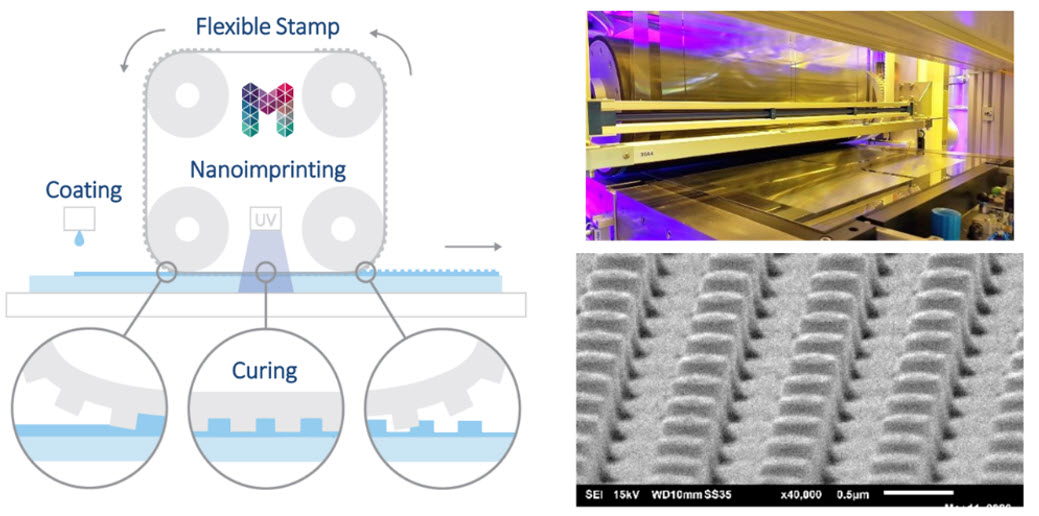 A tiling approach can result in Gen5 R2P nanoimprint tool with integrated UV curing to achieve nano or sub-microfeatures with replication fidelity. The images above are from Morphotonics . To learn more see here
Nanoimprinting can have many uses cases in displays also beyond AR/VR. One example is in development of highly transparent and high conducting metal mesh transparent conductive films. One example is from Meta (Metamaterials) Inc. They have a rolling lithography system.
Here, the UV light is wrapped within a soft rolled-up mask. The rolling nanolithography is used to create sub-micron exposures on a photoresist coated metal substrate. The photoresist is then etched, creating an extremely high-resolution metal mesh.
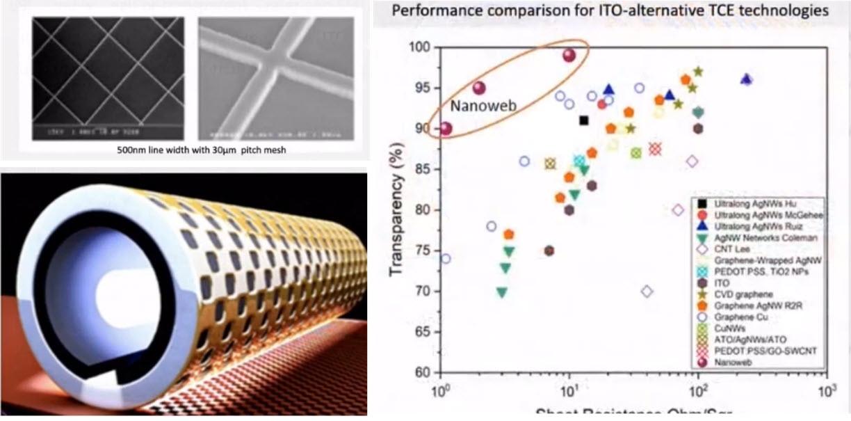 The schematic at bottom left shows the idea of a rolling UV nanolithography by Meta (Metamaterials) Inc. The images at top left show a ultra fine feature metal mesh. The benchmarking charts shows that this process can create ultra transparent and highly conductive films. Currently the web width is 300mm but could be scaled to 1-1.2m. To learn more see here
Fully printed R2R low-cost displays
Printing plays a role also in simple (i.e., segmented) low-cost high-volume displays with applications in smart packaging and beyond.
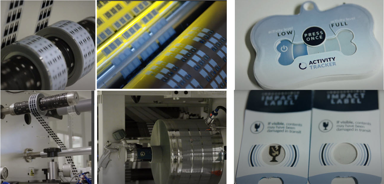
One example is in R2R printed electrochromic displays. A leading player here is Ynvisible. The image set on the left below shows snapshots of full R2R line (printer and converting). This level of automated R2R production is a real progress in the field.
The images on the right images show some application examples. There are numerous applications in smart packaging, IoT sensors, low-cost ubiquitous indicators, etc.
At TechBlick’s next LIVE (online) event you will hear about all the key innovation trends from the most innovative companies. We have leveraged our 15 years of insights into the field of displays and lighting to handpick a fantastic line-up of speakers. With a single Annual Pass, one can participate in this event and all LIVE (online) future events at TechBlick for 12 months. Furthermore, one can access TechBlick’s growing library of on-demand talks from its past events. (KG)
Dr Khasha Ghaffarzadeh is CEO and Founder at TechBlick
Note that for Display Daily readers, the second part will not count towards your monthly free article count.