It takes a minimum of 20 years for a new display technology to go from concept to commercial product, if it ever does.

At SID Display Week 2014 in San Diego, display luminaries celebrated the 50th anniversary of the plasma display panel. It was a bittersweet celebration because it also marked the end of the plasma display as a commercially viable technology. This point was widely discussed by the celebrants, a number of whom were in on the creation of the technology in 1964. In 50 years, the technology had been invented (because a suitable display for the new Plato educational workstation did not exist), rose to be the dominant large-screen display technology, and descended into obsolescence.
In short, by the time a new display technology becomes known beyond the members of the display community who attend the technical paper sessions at SID Display Week, it really isn’t new to the technorati. But analysts know we have entered a more general stage of awareness when venture capitalists and financial advisors start asking them for advice. A recent question: What is the relative market penetration of microLED and OLED? Answer: MicroLED, zero; OLED, more than that. To the person who asked that question, microLEDs are really new.
The Secret is Out
I’ve just given it away, haven’t I? Yes, the new new thing is microLEDs, and the first things we should ask is in what sense are they “micro?” The inorganic LED displays we are used to seeing are large signs. For years, you could choose between displays that had a ptich of 12mm between the LED pixels or a pitch of 6 mm. In the last few years, the lowest pixel pitch available has dropped to 1.2mm and even a bit below 1.0mm from a few suppliers. (Leyard showed 0.7mm at ISE this year – Man. Ed.)
Developmental microLED displays can have a pixel pitch a thousand times less. In part, this is accomplished by doing away with the individual LED packages. Instead, the LED chips are transferred from the semiconductor wafer onto a substrate with backplane, and protected from the environment with a thin film. (This is the general idea, but there are many, many variations on the theme.)
Making the LED chips is standard semiconductor practice, but separating them and transferring them to the substrate is a challenge. The challenge becomes more demanding when you realize that during the transfer the pixel pitch must be expanded by perhaps a 100 times for most direct-view display applications. For an RGB display, the different LEDs must be taken from different wafers because the multi-layer wafer composition is different for each color of LED. And all of this has to be done with at least seven 9’s reliability (99.99999%). (I may be low by one or two 9’s, but you get the idea.)
The RGB problem can be simplified by using only blue LEDs and using red and green quantum dots as color converters, which is why quantum-dot developer, Nanosys, is intensely interested in the technology.
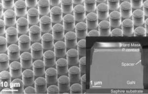
If your application permits, you can avoid a lot of complexity by making your microLED array dirrectly on the wafer, complete with backplane. In this version by the French research lab LETI, the microLED pitch is 10 micrometers. (Photomicrograph: LETI)
If all of this is so difficult, and the developers are concentrating on small direct-view displays, or very small displays for VR goggles, how is it possible that Samsung showed a 146-inch “microLED” display at CES? This modular display was colorful and very bright, and attracted a lot of attention. But Samsung reps would not allow us, or anyone else, to get close to the screen, and what little was said about the technology was confusing. It even turned out that the photo-micrographs near the screen at an analysts-and-media-only event did not even show the structure of the screen in question! The best that a press-and-analysts bull session could do was estimate that pixel pitch must be on the order of 0.1mm. That doesn’t qualify as “microLED.” Maybe it’s a “macro microLED.”
(I have seen data from reliable sources that suggest 125µm x 225µm, which would qualify as miniLED, not microLED which is usually taken as less than 100µm square. The same source quotes 38µm x 58µm as another size that Samsung is working on – Man. Ed.)
In any case, with the promise of greater lifetime, higher luminance, and perhaps better primary color coordinates than OLEDs, microLEDs are a very attractive technology. But there’s a lot of development yet to be done. We haven’t even hit the 20-year mark yet. But you will be able to see some of the developments that have been made at SID Display Week in Los Angeles from May 22 to May 24. – Ken Werner
Ken Werner is Principal of Nutmeg Consultants, specializing in the display industry, manufacturing, technology, and applications, including mobile devices, automotive, and television. He consults for attorneys, investment analysts, and companies re-positioning themselves within the display industry or using displays in their products. He is the 2017 recipient of the Society for Information Display’s Lewis and Beatrice Winner Award. You can reach him at [email protected].