JBD Inc. (Hong Kong, China) is developing a new technology for use in the manufacture of microLED microdisplays.

First, a few words of background information. At the current time, the most common approach used in the production of microLED microdisplays is based on flip-chip technology. This approach uses two wafers. One wafer carries an epitaxial layer of light emitter while the second wafer carries the driver circuitry. In the next step, the wafer carrying the microLEDs is diced into individual chips and flip-bonded on to the wafer carrying the active matrix CMOS IC driver circuitry. Solder bonding is used to make the connections. This process is illustrated in the figure below.
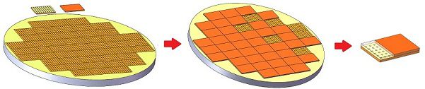 The conventional process used to fabricate microLED microdisplay devices.
The flip-chip approach to manufacturing microLED microdisplays is, however, not without problems.
- Since flip-chip assembly is implemented one substrate at a time, manufacturing throughput is low, making the manufacturing process expensive.
- The thermal mismatch between the LED epitaxial substrate and the silicon substrate with the ICs causes stress to be built in during the bonding process. This, in turn, may cause manufacturing yield loss and long term reliability issues.
- Limitations in the alignment accuracy of bonding equipment makes it difficult to reduce the pixel pitch to a few microns. This limitation is significant because a micron sized pitch is desirable in some potential microdisplay applications.
JBD Goes Monolithic
To address these challenges, JBD is developing a microLED chip fabrication approach based on so-called monolithic hybrid integration technology. The general concept of the technology is to transfer functional microLED epitaxial layers onto silicon IC wafers. In the first step, the wafer containing the microLED epitaxial layer is bonded to the wafer with the IC circuitry. The next step is the removal of the silicon wafer substrate upon which the microLED epitaxial layer was grown. The result is an epi-on-IC structure that is then further processed using standard wafer level semiconductor fabrication processes. The means developed by JBD to produce monolithic hybrid integrated microLED chips is illustrated in the figure below.
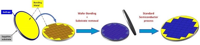 The JDB monolithic hybrid integration microLED chip fabrication process.
The JBD process eliminates the need for the precise alignment required by flip-chip technology. Since the JBD process uses wafer level processing, it is suited for high volume, low cost production. In addition, because JBD technology eliminates the need for the difficult process of bonding pre-defined microLED arrays to the driver ICs, it becomes possible to reduce the size of the pixel pitch.
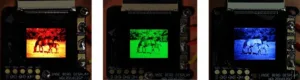
Using JBD’s monolithic hybrid integration technology, monochromatic red, green and blue microLED microdisplays have been successfully prototyped. The figure below illustrates an example of a red, a green and a blue microLED based microdisplay.
Examples of a red, a green and a blue microLED based microdisplay.
These microdisplays displays are 12.8mm in length by 9.6mm in width. They are composed of microLEDs with a device size of 2-3 microns. The device pitch is 5µm. The high pixel density results is a microdisplay resolution of more than 5,000ppi. The brightness of the green active matrix microLED microdisplay was found to be over 500,000 cd/m². This is represented as an improvement of over 500-times compared to existing emissive microdisplays. The current yield of microLED pixels achieved on microdisplays made by JBD is reported as in excess of 99.99%.
During 2019, the company is targeting production of microLED displays with a device size of 1.5-1.7 microns and a pitch of 2.5 microns. If this size is achieved, then the resulting microdisplay would have a resolution of over 10,000ppi. The company is also planning to raise the display brightness to over 100,000 cd/m². The company notes that doing so would ensures the visibility of images even under conditions of intense outdoor lighting which can be on the order of from 5,000 to 8,000 cd/m².
Finally, JBD is also working on full color microLED microdisplays for use in near-eye projection applications. The company explains that “There are essentially two approaches – one using external optics and the other with the hybrid integration technology.” Commenting on the hybrid interaction approach, “we are attempting to use the technology to transfer blank red, green, and blue microLED epi-layers together onto the driver ICs. Vertically aligned, those light-emitting layers, along with the driver ICs, will form a 3D structure. Depending on the LED materials, the driving voltage will be controlled in the range of 3.3V-5V.”
The JBD web site states that “We are seeking more strategic partnerships to upgrade our products and make the commercialization of microLED-based devices as soon as possible.” -Arthur Berman
JBD Inc., Fang Ou, [email protected]