Max McDaniel is Chief Marketing Officer at Applied Materials. He said that there is more change happening now in the industry than ever before, and quick adoption of innovations is essential to capture value.
Applied Materials is the biggest maker of semiconductor and display manufacturing equipment and also makes solar panel equipment. There are four groups, Silicon, Services, Energy and Display divisions. The company makes “really big equipment”.
In display, MacDaniel said that sizes are getting bigger, resolution is increasing, images are getting more vivid and form factors are changing. There is increased revenue coming from addressing these requirements.
High value problems for makers are larger substrates, more layers and more complex structures, new processes and materials and barrier films. Also difficult are flexible substrates and smaller features on transistors.
As panel sizes get bigger, yield can be a bigger problem. It can also be less efficient to make mixed panel sizes on G8 substrates, but equipment scaling is tricky for Gen 11. Resolution increases can make minor defects into “killer” defects so better defect control is essential. Going from a-si to LTPS or Oxide adds mask steps and that can be a challenge.
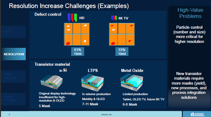 Resolution increases can make minor defects into “killer” defects
In OLED, there are a number of manufacturing challenges including patterning, transistor performance, material lifetime and scaling display sizes up for TV.
In QDs, there are costs in manufacturing and in barriers as well as dealing with toxic materials.
Flexible display manufacture also raises new manufacturing challenges.
In conclusion, overcoming all of these problems with high yield very quickly is a way to help generate profits.