Fujifilm and Imec, a nanotechnology research institute, have worked together to develop a full-colour photoresist OLED. The result ‘paves the way to producing high-resolution and large organic electroluminescent (EL) [OLED] displays and establishing cost-competitive manufacturing methods’, said Fujifilm.
Fujifilm and Imec worked together on a photoresist technology for organic semiconductors in 2013 (Display Monitor Vol 20 No 39). This work enabled sub-micron patterning, without damaging the organic semiconductor materials. It was based on photolithography, capable of high-res patterning on large substrates.
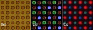
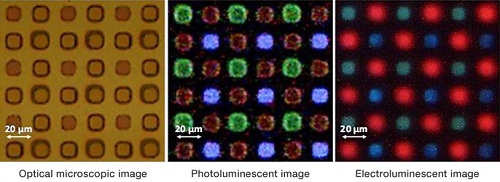 (Left) This OLED array forms a pattern with a sub-pixel pitch of 20µm to achieve 640ppi resolution. (Centre) Image taken with UV illumination on OLED array, confirming that red, green and blue dots emit light separately. (Right) Image taken with voltage applied. All RGB dots confirmed to emit light.
This new work has seen the companies produce a full-colour OLED with the photoresist technology. Red, green and blue materials were patterned, each with a pitch of around 20µm. An array of 40 x 40 dots (640ppi) was created and illuminated with UV rays, to confirm that all of the RGB dots separately emitted light.
Fujifilm and Imec say that the work opens the possibility of using their process in a multiple patterning process. For example, it could be used to add a fourth colour to the RGB matrix.
The work was demonstrated at SID this month.