On July 17th, the Bay Area Chapter of the Society for Information Display meeting hosted a presentation given by Dr. Chris Bower, the Chief Technology Officer at X-Celeprint Limited. At the meeting, Dr. Bower discussed in detail his company’s development work on the use of an elastomer stamp to manufacture microLED displays. The company calls this technology Micro-Transfer Printing (μTP).
 Dr. Chris Bower, CTO at X-Celeprint (Credit: X-Celeprint)
While microLEDs have the potential to be the best display technology over a very wide range of sizes and applications in terms of image quality, energy efficiency, colorimetry, etc., they pose formidable cost and manufacturing problems. These benefits and problems were discussed at the recent QLED & Advanced Display Summit (ADS), hosted by Insight Media and sponsored by Samsung. (See MicroLEDs at the ADS – Part 1 and MicroLEDs at the ADS – Part 2 – Subscription required) For a 4K TV, it is necessary to transfer about 25 million LED die from the red, green and blue epitaxial wafers to a backplane with roughly 1µm accuracy and a 99.99999% or higher yield after repair. This must also be done at a reasonable manufacturing speed. For example, a pick-and-place technique that transferred 1 die/second that operated 24/7 would take about 288 days to populate a single 4Kpanel. That’s not a realistic production rate.
At the ADS, 14 different techniques from 27 companies or universities were discussed that would to speed up this process. While the elastomer stamp process from X-Celeprint was mentioned, it was not discussed in any detail. Besides X-Celeprint, it was reported that ITRI (Industrial Technology Research Institute of Taiwan) and KIMM (Korea Institute of Machinery & Material) were also working on their versions of the elastomer stamp process. Development of the process used at X-Celeprint was started by Professor John Rogers at the University of Illinois at Urbana-Champaign in the mid 2000’s and was spun out to the company Sempruis in 2006, with the intention of using it to make solar panels. X-Celeprint was formed and acquired the bankrupt Semprius intellectual property in 2013. The X-Celeprint business plan is to develop and license advanced assembly solutions based on the µTP technology. The technology can transfer not just LED die, but other objects as well. For example, Dr. Bower discussed transferring small silicon drive circuits for microLED pixels as well as the die themselves.
X-Celeprint transfer stamp process
 Operation of an elastomer stamp (Credit: X-Celeprint)
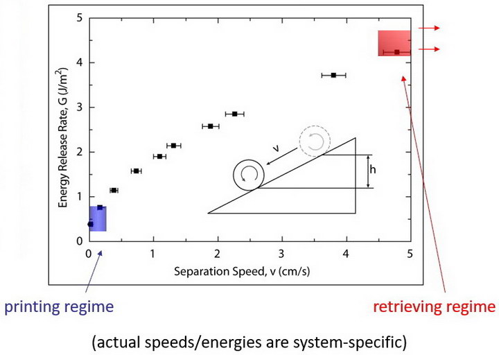
The principal of operation of an elastomer stamp is shown in the figure. When the separation speed between an elastomer material such as silicone and the object it is touching is fast, the binding energy between the stamp and the touched surface is relatively high. For example, if the stamp is touching a properly prepared LED epitaxial wafer and removed quickly, this high binding energy means the die stick to the stamp and are removed from the wafer (retrieving regime). When the stamp with the die attached to it presses down on a properly prepared substrate and then removed slowly, the low binding energy allows the die to remain on the substrate (printing regime). In practice, the X-Celeprint stamp is flat, not cylindrical as shown in this figure.
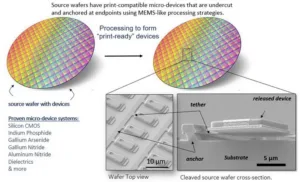
Wafer preparation for elastomer printing. (Credit: X-Celeprint)
This figure shows the preparation needed for a LED epitaxial wafer or other wafer before the LED die can be transferred by an elastomer stamp. This preparation involves undercutting each die to be transferred using MEMS-like processing steps that leave the die attached to the wafer only by a small tether attached to an anchor on the source wafer. When the stamp presses down on the wafer, the die adheres to the stamp. When the stamp is lifted quickly, the high binding energy between the stamp and the die means the die remains adhered to the stamp and the tether breaks.
 Each stamp picks up multiple microLEDs (Credit: X-Celeprint)
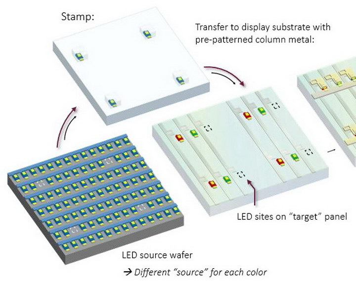
Direct view microLED displays require much larger spacing on the final display than on the source epi wafer. X-Celeprint achieves this by designing its stamp to pick up only a small fraction of the microLEDs on the wafer at a time. In the example image, the stamp picks up every 8th microLED horizontally and every 4th vertically for transfer to the display substrate. This increases the center-to-center microLED spacing by a factor of 8x horizontally and 4x vertically in the example. This would require a total of 32 stamp transfers to move all the die from the source wafer to the target substrate. While the sample image shows transferring 4 die with each stamp, typically a much larger number would be transferred with on stamp – as many as 10,000 or more at a time, depending on the system design. This technique has been shown to be able to transfer up to 60K die at a time. After the die are transferred to the target panel, X-Celeprint uses a stamp cleaning step before going back to pick up the next batch of die from the source wafer.
 Stamp master and the final production stamp (Credit: X-Celeprint)
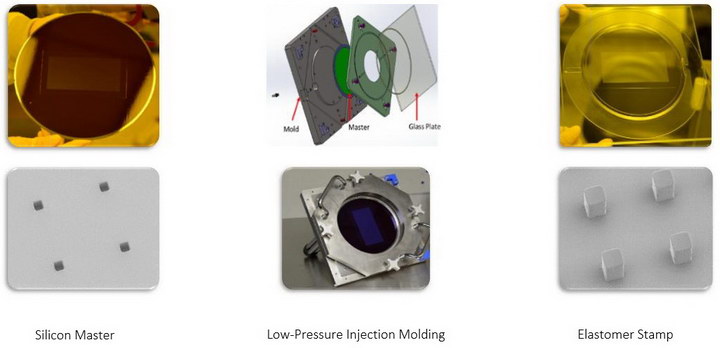
If you want to transfer 10,000 die at a time, you must have an elastomer stamp with 10,000 die-sized plateaus on it, with each plateau located within about 1µm of its target location. X-Celeprint makes its masters using silicon wafers and photolithographic technology, a process that can easily achieve this level of accuracy. The stamp master is then used in a low-pressure injection molding system to produce the stamps used in production. According to Dr. Bower, each stamp can be used at least 5,000 times and X-Celeprint has used its stamps 35,000 times without problems. When a stamp needs to be replaced, a new stamp is made from the master by the relatively inexpensive low-pressure injection molding process. While making the master is more expensive, typically it would only need to be done once for each microLED display design.
After all the RGB microLED die are transferred, along with the small ASIC, if used, the next step in the manufacturing process is metallization to connect all the die to the substrate and drive circuitry.
X-Celeprint Manufacturing Strategies
Dr. Bower discussed X-Celeprint manufacturing strategies both toward the end of his talk and in the Q&A session that followed his formal presentation. He said the smallest die X-Celeprint is working with are 3µm sized. He added that X-Celeprint is targeting current display types such as TV systems and smartphones and smaller die such as 1µm are not needed in these systems. X-Celeprint is planning on developing and licensing the manufacturing technology and does not plan on becoming a display supplier itself.
One of the major issues with the X-Celeprint process, or any manufacturing process for microLED displays, is yield. The first yield issue is with the epi wafers themselves. A stamp process, and most other processes under development for microLED displays, uses every die on the wafer, including every bad die. Dr. Bower says this is not, in fact, a real issue and most of the yield issues at X-Celeprint come from the X-Celeprint processes, not from the epi processes.
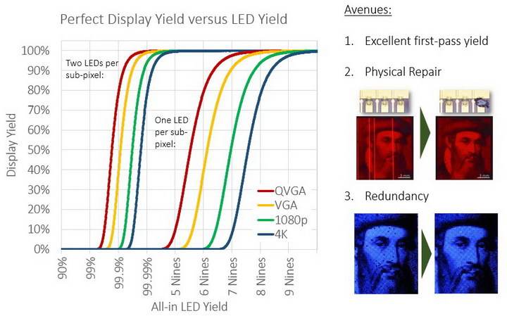 Yield requirements for various display resolutions (Credit: X-Celeprint)
Dr. Bower said the company in a test run achieved about 99.98% red die yield and 99.95% yield for green and blue die. This is a far cry from the 8-9’s or 9-9’s needed for a 4K TV process that would be effectively defect-free. He says there are two approaches X-Celeprint is pursuing to produce commercially viable panels.
First is redundancy – instead of one die of each color per pixel, two die can be used. If the primary die is good, it is used. If not, the secondary die at the pixel is used. A yield of 99.99%, X-Celeprint’s near-term goal, turns into a yield of 8-9’s (99.999999%), and roughly 80% of 4K panels will be defect free and repair is not needed for those panels. The other 20% of the panels will likely only have one or two bad pixels requiring repair. This redundant approach has a major down-side: it essentially doubles the material and transfer cost for a microLED display. These material and transfer costs are a major part of a direct view microLED display cost, as discussed by several speakers at the ADS.
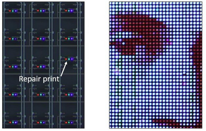 Left: Repair of a bad pixel by inserting a new RGB die assembly adjacent to the bad location. Right: the offset of the repaired pixel (in the nose, on the right side of the image) would not normally be visible. (Credit: X-Celeprint)
The alternative is to use a single die per color per pixel and repair the bad pixels. X-Celeprint is developing processes that inserts either a new die or a new RGB die assembly at a location adjacent to the location of the bad die or pixel. This results in the repaired die or pixel being in a location slightly offset from the original location, as shown in the image. Dr. Bower said that in a high-resolution display at normal viewing distances, the offset of the die or pixel would not be visible.
Dr. Bower said with the current yield levels (4-9s) he believes the redundant approach is more cost-effective than the approach of using a single die per pixel and repairing a large number of bad pixels. Even with the redundant approach, some repair is likely to be needed, however, which is why X-Celeprint is developing repair processes. As yields increase beyond 99.99% good die on the display backplane, the cost trade off between redundant die and repair will be pushed in the repair direction.
I asked Dr. Bower during the Q&A if particles were released during the fracture process when die are removed from the epi wafer and did these particles cause a yield problem. His answer was yes, particles were released and yes, they affected down-stream yield. He said the main problems caused by these particles were during the metallization step. He didn’t give a specific number for the yield problems caused by these particles, but he did say that at the 4-9’s yield level, they were on the Pareto analysis of problems that need to be solved to reliably reach the target yields.
 The X-Celeprint team in North Carolina (Credit: X-Celeprint)
X-Celeprint is headquartered in Cork, Ireland at the Tyndall National Institute. Micross, a wholly owned subsidiary of X-Celeprint, is based in Research Triangle, North Carolina. It is the North Carolina group that is developing the Micro-Transfer Printing technology for microLED displays. –Matthew Brennesholtz